
Abstract
Deep submicron technology faces challenges arising from the demand for smaller integrated circuits (ICs). One major challenge is interference caused by interwire capacitance. As the distance between wires decreases, coupling capacitance can become comparable to or exceed the load capacitance, creating delay and power-dissipation problems. Encoding techniques address this problem by mapping data words to codewords that avoid harmful transitions. Forbidden-pattern-free (FPF) and forbidden-transition-free (FTF) techniques exclude patterns associated with high crosstalk. The study discusses FPF as an implementation option and reports a 17% improvement in system performance, while recognising the area overhead introduced by codec design. Mapping data words to codewords remains difficult because of the nonlinear structure of crosstalk avoidance codes. Propagation delay and power consumption are important design concerns for buses in deep submicron (DSM) systems. Coupling between adjacent wires can produce crosstalk, noise, delay and increased power consumption. This paper examines an FPF encoder and decoder intended to improve bus performance by avoiding harmful interwire transition patterns.
Keywords: Deep Submicron Technology (DSM), Integrated Circuits (IC), Interwire Capacitances, Forbidden Pattern Free (FPF), Forbidden Transition Free (FTF), Mapping Techniques, Nonlinear System, Propagation Delay, Area Overhead.
Introduction
Deep submicron technology refers here to microchip fabrication with feature sizes below 0.25 micrometres [1]. It has enabled faster microprocessors and memory chips [2], including microprocessors operating at clock rates of several gigahertz. Very-large-scale integration (VLSI) circuits have benefited from these increases in speed and integration density [3]. However, smaller transistors and interconnects, lower supply voltages and higher operating frequencies can increase susceptibility to transient and intermittent faults. Coupling capacitance contributes to crosstalk noise, power loss, propagation delay and logical errors on on-chip buses. Capacitive interactions in DSM systems are associated with several signal-integrity problems [4]. Opposing transitions on neighbouring wires can intensify coupling effects [5]. Wire propagation delay also affects data-transfer reliability and overall system performance. Two important consequences of increased coupling capacitance are crosstalk noise and crosstalk latency [6]. As feature sizes shrink, coupling becomes increasingly significant [7]. The proximity of neighbouring wires and their increasing aspect ratios contribute to these effects in densely integrated devices [8].
Improving an IC’s operating speed requires attention to the resistance–capacitance (RC) delay of its interconnects. Mutual inductance and coupling capacitance contribute to crosstalk noise [9]. Inductive coupling affects signal integrity and latency and can be addressed through shielding and buffering. Capacitive crosstalk is also influenced by wire spacing and sizing. Other measures include changing victim and aggressor driver sizes, introducing shields and inserting buffers [10]. Active shielding uses an additional driver to generate a counteracting signal, while passive shielding separates signal lines with a shielding conductor. Increasing the spacing between neighbouring wires can reduce coupling and crosstalk noise [11], although it may increase chip area and interconnect length. Low-swing signalling reduces the voltage swing and associated switching energy, but may require receiver circuitry to restore the signal. Crosstalk mitigation can also involve intentional timing skew at transistor level and wire spacing, shielding or repeater insertion at physical level [12]. These methods introduce overhead in network-on-chip (NoC) systems. Register-transfer-level (RTL) approaches, including crosstalk avoidance codes (CACs), provide an alternative way to control harmful transitions [13].
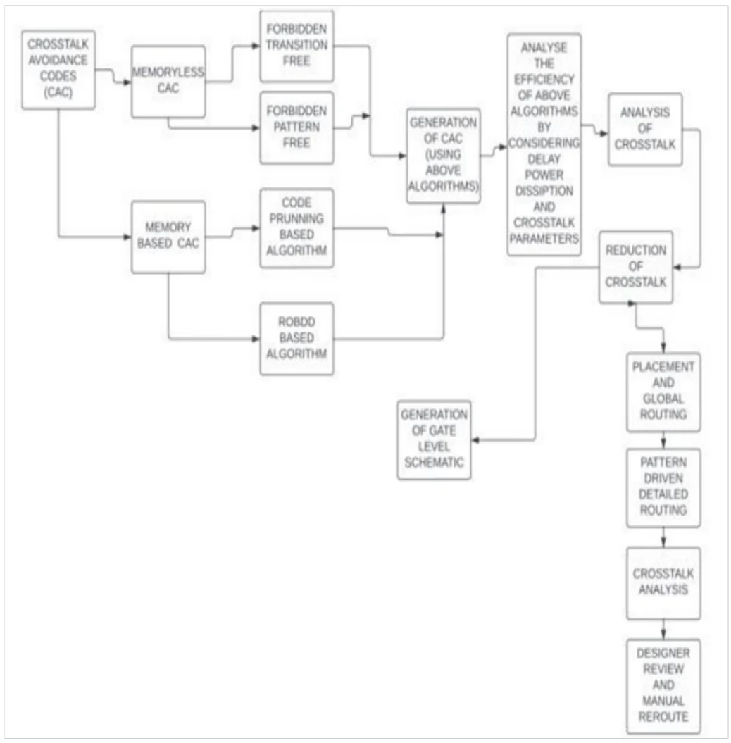
Crosstalk avoidance codes reduce the occurrence of signal transitions or patterns associated with interference [14]. Avoiding these patterns can reduce the effects of interwire coupling, improve signal integrity and lower power consumption. FPF and FTF are two memoryless approaches discussed in this study [15]. Both seek efficient crosstalk avoidance with limited coding overhead. The paper focuses on FPF coding and compares its implementation requirements with those of FTF. The central design issue is how to obtain useful delay reductions without excessive costs in wiring, logic area or codec latency.
The study presents the following contributions:
An FPF coding approach intended to reduce crosstalk and improve the signal-to-noise ratio (SNR).
An algorithm for generating FPF codewords for the 3C case, with an encoder and decoder implemented in Verilog.
A simulation-based examination of encoding and decoding, with claimed improvements in throughput and bit-error performance.
Literature Review
In 2021, Vinodhini et al. [16] suggested a coding method called Crosstalk Aware Transient Error Correction (CATEC) to enhance communication reliability and lower power use in NoC connection architecture. The approach aims to reduce flicker-related self and coupling transitions and rectify error patterns containing one or two temporary error bits, thereby achieving a low-power Network-on-Chip (NoC) connection and mitigating crosstalk. This inquiry strives to tackle the underlying obstacles in the development of NoC interconnects, encompassing the simultaneous fulfilment of the criteria for efficiency and energy usage in the System-on-Chip (SoC), whilst also taking into account the element of reliability. By reducing flicker-related self and coupling transitions and rectifying error patterns with one or two temporary error bits, the approach yields a low-power NoC connection and effectively prevents crosstalk. The suggested CATEC approach is not contrasted with any currently used techniques in the research. A future study is recommended in this research to examine the viability of using the CATEC approach to more SoC interconnects and to assess how well the suggested technique performs in the presence of process changes.
In 2019, Bamberg et al. [17] proposed a novel approach to transfer current 2D crosstalk avoidance codes onto rectangular or hexagonal TSV configurations, therefore reducing crosstalk in 3D integrated circuits. The suggested method lowers crosstalk in metal wire and TSV buses while essentially maintaining power consumption. This work introduced 3D CAC to overcome existing limitations. The suggested method gets over the drawbacks of the 3D crosstalk avoidance codes that are already in use. Simulations are used to assess the suggested approach, and real-world performance may vary.
In 2020, Terapasirdsin and Kiattisin [18] suggested a strategy for reducing crosstalk energy in VLSI circuit design by taking the signal transition into account. To get the optimum value in signal lines that are structured such that there is less noise, the shuffled frog leaping algorithm (SFLA) is utilized. For comparison, the research also looks at other optimization strategies including simulated annealing (SA) and ant colony optimization (ACO). The approach uses an efficient optimisation method (SFLA) to find the optimum value among signal lines that are organized in a way that produces the least amount of noise. Not all VLSI circuit designs may be compatible with the suggested method. The article recommends that various objectives be used in the future for more testing.
In 2022, Taali et al. [19] proposed a Joint Capacitive and Inductive Crosstalk Avoidance Code (JCI-CAC) algorithm to avoid crosstalk errors in communication buses by taking into account both capacitive and inductive coupling effects. The suggested approach offers a novel numerical system for data encoding with little computing cost while taking into account capacitive and inductive coupling effects. The comparison records a delay value of 665, equivalent to the state-of-the-art method, as a limitation.
In 2020, Wang et al. [20] suggested a chip partition optimization platform (POP) to lower crosstalk noise and power loss in silicon-photonic multistage switching fabrics, which can enhance signal integrity. The platform can cut down on waveguide crossings and lower the distance that optical signals must travel across a semiconductor. The goal of the study is to enhance the functionality of a chip partition optimization platform (POP) utilized in data centers to optimize inter-node networks. This platform incorporates three orthogonal optimization techniques: local optimization, vertical chip partition, and horizontal chip partition. By employing these techniques, the POP effectively reduces power loss and mitigates crosstalk noise in silicon-photonic multistage switching fabrics, enhancing signal integrity. Small-scale switching fabrics may not be suited for the proposed platform.
In 2020, Mondal et al. [21] suggested a technique for on-chip interconnects in 2D and 3D integrated circuits to assess and optimize crosstalk noise. The technique uses a crosstalk noise and modified routing algorithm and model to minimize crosstalk. The suggested methodology of Maximum Ratio Combining (MRC) harbors the capability to efficiently diminish crosstalk noise and present ideal routing resolutions in both two-dimensional (2D) and three-dimensional (3D) integrated circuits (ICs) with negligible computational load. This research also suggests the possibility of conducting future investigations into crosstalk noise within the power supply networks of 2D and 3D ICs. The primary goal is to ascertain and diminish the disruption induced by crosstalk in the interconnections within integrated circuits that possess either two-dimensional or three-dimensional characteristics.
In 2020, Badugu [22] examined the implications of linked interconnect crosstalk for ternary logic applications. The research illustrates that the utilization of copper-multilayer graphene (Cu-MLG) interconnects accompanied by MLG barriers reduces the occurrence of crosstalk effects, power dissipation, and power delay product (PDP) in contrast to conventional Cu interconnects. The proposed interconnects will be driven by a conventional ternary inverter (STI) based on GNRFETs. This study demonstrates the performance gains of Cu-MLG interconnects over Cu interconnects using findings from industry-standard HSPICE simulations.
In 2020, Sayil et al. [23] suggested a fresh approach to reducing crosstalk noise that is based on a cutting-edge transmission gate design. A unique transmission gate design serves as the foundation for the new crosstalk noise reduction technology suggested in this study. The approach includes altering the gate bias of the pass transistors to regulate the crosstalk pulse width that has to be reduced. The “driver sizing” approach and the “basic transmission gate” technique are compared to the suggested methodology in terms of area and delay overheads in this study. There is very little circuit layout adjustment necessary.
In 2019, Jamshidi and Fazeli [24] proposed the use of magnetic-based Driver-Receiver circuits and current mode signaling for the creation of an interconnect that is both ultra-low power and reliable. In order to ensure crosstalk robustness, power consumption, and latency are taken into consideration, a suggested link is put forward. The Pulsed Current Mode Interconnect (PCMI) technique was employed in this investigation with the principal aim of diminishing delay, power consumption, and crosstalk. The presence of hysteresis in the system was determined to bestow a notable benefit in relation to noise resilience, as underscored in this scholarly article.
In 2021, Shirmohammadi et al. [25] proposed an innovative crosstalk avoidance code (CAC) that employs three symbols, unlike traditional binary CACs, which use only binary symbols. This novel CAC, known as the Summation-based tri-value CAC (ST-CAC), effectively minimizes the worst-case latency on bus lines and can be successfully applied to lines with any arbitrary channel width. Additionally, the main goal of this study revolves around eliminating crosstalk in the channel. The significant advantage of the ST-CAC lies in its utilization of three symbols to represent the data on the bus, thereby enabling a reduction in the number of lines required in communication channels. Table 1 shows the state of the art in existing crosstalk reduction methods.
Table 1. Comparison of several existing crosstalk reduction techniques
Year & Author | Method used | Aim | Advantages | Disadvantages |
2021, Vinodhini, et al [16] | CATEC | Handle the important NoC connection design concerns, | Corrects error patterns Reduce power consumption | It does not compare the proposed technique with existing methods |
2019, Bamberg, et al [17] | 3D CAC | Crosstalk avoidance in 3D integrated circuits | Reduce crosstalk with unaffected power consumption. Requires less hardware | Real-world performance may differ |
2020 Terapasirdsin and Kiattisin [18] | SFLA | to get the optimum value in signal lines that have been organized such that there is less noise. | Minimal noise | Some VLSI circuit designs might not be compatible with the suggested method. |
2022, Taali, et al [19] | JCI-CAC | To guard against crosstalk issues in communication buses. | Cross talk faults prevented. Power consumption reduced. | It has a 665-delay equivalent to the SOTA method, which is listed as a limitation. |
2020, Wang, et al [20] | POP | in order to optimize the integrity of signals, the goal is to reduce power loss and minimize the interference caused by crosstalk noise in multistage switching fabrics that utilize silicon-photonic technology. | Less power loss. Low crosstalk noise Improved signal integrity. | For small-scale switching fabrics, this method might not be appropriate. |
2020, Mondal, et al [21] | MRC algorithm | To assess and diminish the interference noise between on-chip interconnects in 2D and 3D integrated circuits. | Minimize estimated crosstalk noise. termination of crosstalk noise under high-frequency operation Accurate noise assessment | The paper does not discuss the limitations |
2020 Badugu [22] | GNRFET | In order to address the consequences of crosstalk, power loss, power delay product (PDP), and energy-delay product (EDP) in relation to traditional Copper interconnections, it is imperative to employ customized tactics. | Compared to conventional Cu interconnects, Cu-MLG interconnects demonstrate a higher level of compatibility when employed in conjunction with ternary logic integrated circuits. | The creation of Cu-MLG interconnects is not covered in the study. |
2020 Sayil, et al [23] | TG | To put forth a unique transmission gate design with minimal space and performance overheads as a new way for reducing crosstalk noise in integrated circuits. | Requires little circuit-layout modification. Feasible for reducing noise caused by crosstalk at the post-route design stage | Depending on the unique qualities of the integrated circuit being developed, the proposed methodology’s efficacy could vary. |
2019 Jamshidi and Fazeli [24] | PCMI | To reduce crosstalk, power consumption, and latency | The hysteresis attribute makes the system far more resistant to noise. Less power consumption | The constraints are not covered in the reviewed comparison. |
In 2021, Shirmohammadi, et al [25] | ST-CAC | To remove the worst channel transition patterns caused by crosstalk | Data on the bus is encoded using three symbols, allowing to cut several lines in communication channels. | No limitations were discussed in the reviewed comparison. |
Proposed Methodology
This research examines FPF coding for reducing crosstalk and improving SNR in DSM technologies. The described simulation approach considers channel length, data speed and crosstalk conditions. An algorithm generates FPF codewords for the 3C case, and Verilog is used to implement an encoder and decoder. Simulation trials then examine the operation of the proposed encoding and decoding method.
Global bus delay is a design concern in deep submicrometre SoC architectures. As feature sizes shrink, gate delays decrease, making interconnect delay increasingly important. The manuscript represents the delay on an m-bit bus using Equation (1).

Here, τ0 is the transition delay of a single wire, λ denotes the adjacent-wire coupling-capacitance ratio, and Δi represents the transition term for the ith wire, as used in Equation (1).
Crosstalk delay can be several times the delay of an isolated wire and can therefore dominate bus latency. Its significance increases as feature size decreases and the coupling ratio λ rises. Equation (1) describes the delay dependence on neighbouring transitions. Avoiding patterns associated with high delay can reduce latency, although an encoded bus may require additional wires. The coding rate expresses the relationship between the number of data bits and the number of wires used, allowing the associated redundancy to be assessed. CAC designs offer different trade-offs between coding rate and worst-case delay reduction. The following sections describe the FPF approach.
Forbidden Pattern Free Coding
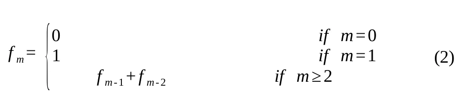
A forbidden-pattern-free code avoids specified patterns on any three consecutive bus bits. For example, “100110” is an FPF codeword, whereas “10111” is not. The manuscript expresses the maximum codeword cardinality in terms of fm+1, where fm is the mth member of the Fibonacci sequence. Equation (2) gives the recurrence used in the analysis.
3C FPF Crosstalk Avoidance Codes
The 3C FPF approach adds bits to the transmitted representation to exclude harmful 3C and 4C transition patterns. FTF and FPF are two coding approaches used to address channel crosstalk. This study focuses on an FPF-CAC encoder and decoder intended to reduce latency and power consumption. The encoder maps data words to valid codewords so that harmful adjacent-wire transitions are avoided. Coupling capacitance between neighbouring wires is the principal mechanism considered. Changes from 0 to 1, or from 1 to 0, can interact with neighbouring transitions and produce crosstalk. The decoder reverses the mapping to recover the transmitted data.
Fibonacci Representation and Codec Design
FPF coding can be used to exclude the 3C and 4C crosstalk classes. Data-word-to-codeword assignments may be changed provided that the decoder can reverse the mapping. When the codebook size is not a power of two, some data words may have more than one available codeword, offering flexibility in codec design. For a constrained bus width, the mapping can be selected to improve speed, area or both. However, the number of possible mappings grows rapidly as bus width increases. The manuscript discusses codec widths ranging from 3 to 121 bits and notes the growth in the number of required two-input gates. Extending a mapping from a narrow bus to a wider one is difficult because CACs have a nonlinear structure. Alternative memoryless codec designs include bus partitioning, in which a wide bus is divided into smaller groups, typically containing three to five bits. An exhaustive search can identify efficient mappings for each group. This method nevertheless introduces overhead for group boundaries and for controlling crosstalk between groups. The Fibonacci numeral system provides another representation relevant to CAC design, as shown in Equation (3).

In Equation (3), v is the represented value, fk is the kth Fibonacci number, and dk is a binary digit taking the value 0 or 1.
Equation (4) gives the additional Fibonacci relationship used in the manuscript.

The manuscript relates the represented range to [0, fm+2] and describes fm+2 distinct values for m-bit Fibonacci vectors.
FPF Encoder
The encoder implementation is based on Equation (3). It transforms an n-bit input through a sequence of m−1 stages, while the decoder reverses the bus codewords to restore the original binary word. Equation (5) gives the arithmetic decision performed at an encoder stage.

The remainder is updated according to Equation (6).

Each stage produces a bit dk and a remainder rk. At the most significant stage, rk+1 is the input value to be encoded; at later stages, it is the remainder passed from the preceding calculation. For even m, the described implementation uses a comparator, an adder and a 2:1 multiplexer. For odd m, it requires an adder and multiplexer because the subtraction operation also performs the comparison. Figure 1 shows the m-bit FPF-CAC encoder.
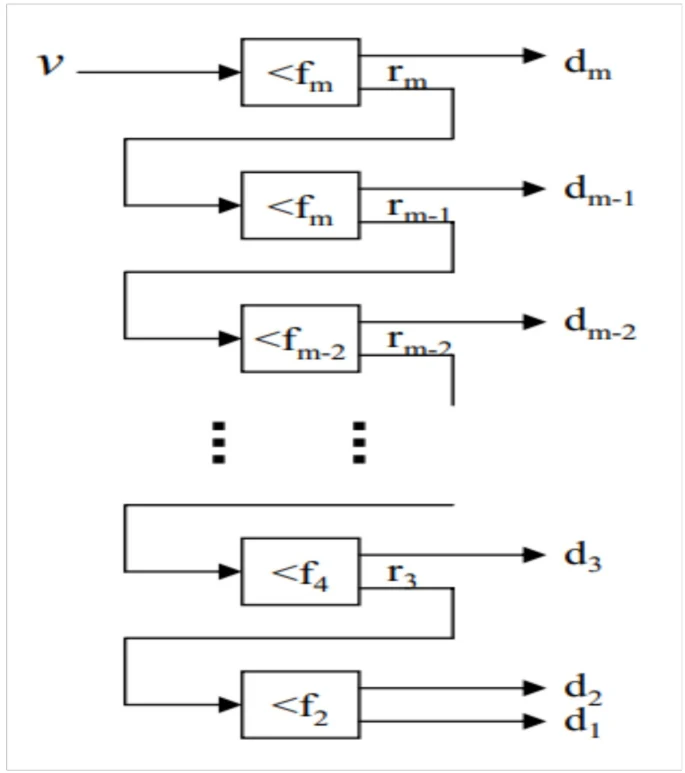
Figure 1. Structure of FPF CAC Encoder
FPF Decoder
Figure 2 shows the structural block diagram of the FPF decoder. Although the diagram contains multiplier symbols, the implementation does not require general multiplication or AND operations for every term. Multiplication of a single-bit input dj by a constant fj is implemented by routing that bit to the nonzero positions of the constant. The m inputs to the summation block have different widths. The most significant input has the width associated with fm, while the two least significant inputs each contain one bit. The computational complexity is described as approximately O(m²/2).
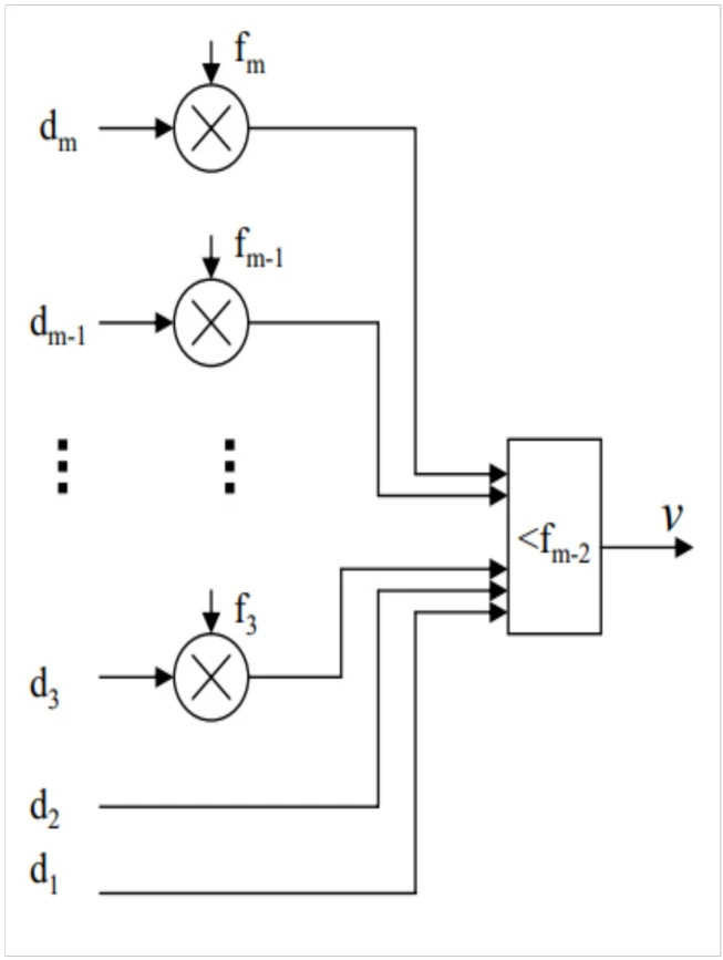
Figure 2. Block diagram of FPF-CAC decoder
The encoder and decoder seek to avoid harmful patterns such as “101” and “010”. The following algorithm maps three-bit data words to four-bit codewords. Table 2 records the use of one’s-complement and two’s-complement operations for the eight possible input words. The mapping assigns the two’s-complement operation to “010” and “101” and the one’s-complement operation to the other six inputs.
Table 2. The methods used for converting data words into codewords
Data words | method | ||
d1 | d2 | d3 | |
0 | 0 | 0 | 1’s complement |
0 | 0 | 1 | 1’s complement |
0 | 1 | 0 | 2’s complement |
0 | 1 | 1 | 1’s complement |
1 | 0 | 0 | 1’s complement |
1 | 0 | 1 | 2’s complement |
1 | 1 | 0 | 1’s complement |
1 | 1 | 1 | 1’s complement |
Table 2 summarises the complement operation assigned to each input word. Algorithm 1 describes generation of the fourth code bit and the additional pattern checks.
Algorithm 1: 3 to 4-bit codeword generation |
Data words: d1, d2, d3 For i = 1 to i = 3 If d1 d2 d3 is not a FPF vector c1 c2 c3 = 1’s complement of (d1, d2, d3) else c1 c2 c3 = 2’s complement of (d1, d2, d3) end if end for For i = 4 If there is a repeated pattern, then Ci = (di – 3) XOR (di – 2) Elsif c1c2c3c4 is an FPF vector C1 C2 C3 C4 = d1 d2 d1 d2 end if end for |
Algorithm 1 generates a four-bit codeword from a three-bit data word. Table 3 gives the resulting FPF codec mapping for inputs d1, d2 and d3. A three-to-four-bit encoder performs the transformation at the transmitter. A four-to-three-bit decoder then applies the inverse mapping at the receiver to recover the original data word.
Table 3. Generation of 4-bit code words for 3-bit data words using FPF
Data words | Code words | |||||
d1 | d2 | d3 | C1 | C2 | C3 | C4 |
0 | 0 | 0 | 1 | 1 | 1 | 0 |
0 | 0 | 1 | 1 | 1 | 0 | 0 |
0 | 1 | 0 | 0 | 0 | 1 | 1 |
0 | 1 | 1 | 1 | 0 | 0 | 1 |
1 | 0 | 0 | 0 | 1 | 1 | 1 |
1 | 0 | 1 | 0 | 1 | 1 | 0 |
1 | 1 | 0 | 1 | 1 | 1 | 1 |
1 | 1 | 1 | 0 | 0 | 0 | 0 |
Before transmission, a k-bit message is mapped to an m-bit CAC codeword to avoid transition patterns associated with large crosstalk delays. The additional coded bits introduce wiring redundancy. The receiver accepts the encoded word and applies the corresponding decoder to recover the original k-bit message within the described communication sequence.
Results and Discussion
This section presents the Verilog simulation of the FPF encoder and decoder. The transmitter maps three-bit data words to four-bit codewords, while the receiver performs the inverse transformation. Figure 3 shows the RTL schematic of the FPF-CAC implementation. The encoding stage is intended to avoid unwanted transition patterns on adjacent interconnects and thereby reduce crosstalk in DSM systems. The simulation material illustrates the logical encoding and decoding operations.
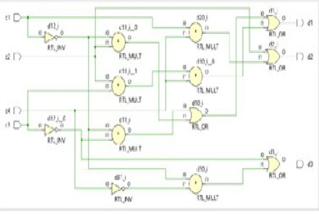
Figure 3. RTL schematic of FPF-CAC
Simulation of the FPF Encoder
The three-to-four-bit encoder converts each three-bit input word into a four-bit codeword. The input sequence ranges from “000” to “111”. Within that sequence, “010” and “101” contain the alternating patterns of interest, while the other six words belong to the remaining pattern group. Table 2 assigns complement operations to these groups, and Table 3 specifies the resulting codewords. The fourth code bit is generated through the XOR and pattern-checking steps in Algorithm 1. Verilog HDL is used to simulate the encoder. Figure 4 shows its output waveform. For the input d1 = 0, d2 = 1 and d3 = 0, the reported output is C1 = 0, C2 = 0, C3 = 1 and C4 = 1. For d1 = 1, d2 = 0 and d3 = 1, the reported codeword is C1 = 0, C2 = 1, C3 = 1 and C4 = 0.
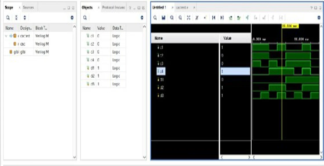
Figure 4. The output waveform of the FPF encoder
Simulation of the FPF Decoder
The four-to-three-bit decoder reverses the encoder mapping and converts each received codeword into its corresponding three-bit data word. Verilog HDL is used to implement and simulate the decoding operation. The encoder changes the transmitted representation to avoid harmful patterns, and the decoder restores the original information. Figure 5 presents the supplied decoder simulation waveform. The approach is intended to reduce crosstalk and propagation delay in communication, with a corresponding reduction in power consumption. These benefits depend on the encoded transition behaviour and implementation overhead.
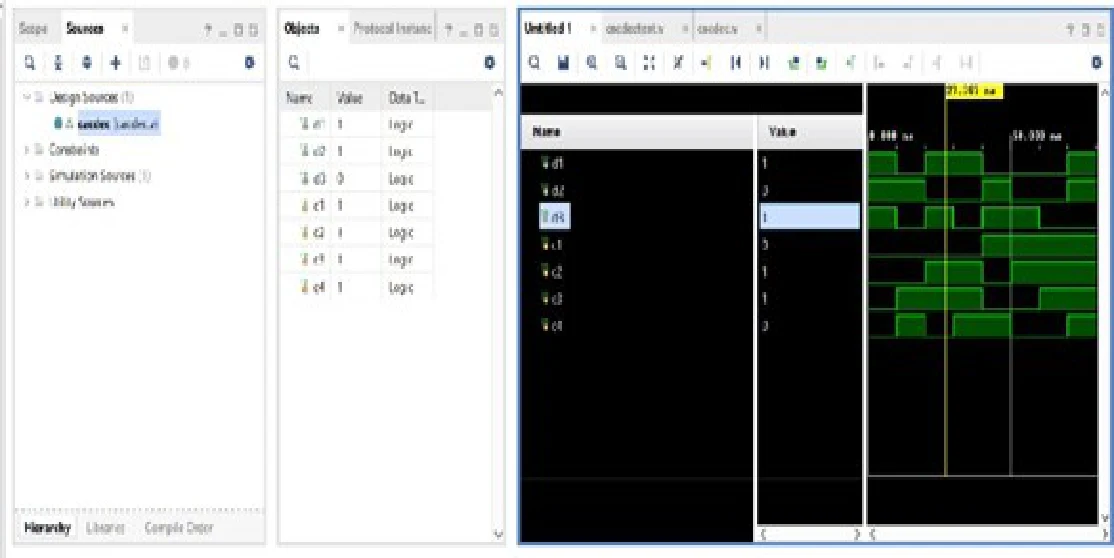
Figure 5. The output waveform of the FPF decoder
The manuscript reports that the FPF encoder and decoder reduce information-transmission latency by 40%. It also describes benefits in the trade-off between additional area, transmission delay and power dissipation compared with conventional approaches. The supplied simulation figures illustrate the codec operation associated with these reported findings.
Conclusion
As VLSI feature sizes decrease, capacitance between neighbouring wires on the same metal layer becomes increasingly important relative to wire-to-substrate capacitance. This paper examines FPF-CAC encoding as a means of reducing adjacent-wire crosstalk and improving bus speed. The proposed codec converts three-bit data words into four-bit codewords at the transmitter and reverses that transformation at the receiver. Avoiding harmful transition patterns is intended to reduce propagation delay and switching-related power consumption. The study reports a 40% latency reduction for the proposed method. Its Verilog simulations demonstrate the encoding and decoding operations used in the design.
References
Kumar, S., Bhushan, P., Pandey, M. and Bhattacharya, S., 2019. Additive manufacturing as an emerging technology for fabrication of microelectromechanical systems (MEMS). Journal of Micromanufacturing, 2(2), pp.175-197.
Di Mascio, S., Menicucci, A., Gill, E., Furano, G. and Monteleone, C., 2021. On-board decision making in space with deep neural networks and risc-v vector processors. Journal of Aerospace Information Systems, 18(8), pp.553-570.
Soumya, N., Kumar, K.S., Rao, K.R., Rooban, S., Kumar, P.S. and Kumar, G.N.S., 2019. 4-bit multiplier design using cmos gates in electric VLSI. International Journal of Recent Technology and Engineering, 8(2), pp.1172-1177.
Joy, T. and George, S.N., 2020, January. Power optimization Techniques in High Frequency Processor Blocks. In 2020 Fourth International Conference on Inventive Systems and Control (ICISC) (pp. 1-6). IEEE.
Hurshkainen, A., Mollaei, M.S.M., Dubois, M., Kurdjumov, S., Abdeddaim, R., Enoch, S., Glybovski, S. and Simovski, C., 2020. Decoupling of closely spaced dipole antennas for ultrahigh field MRI with metasurfaces. IEEE Transactions on Antennas and Propagation, 69(2), pp.1094-1106.
Gugulothu, B., Naik, B.R. and Boodidha, S., 2019, April. Modeling of capacitive coupled interconnects for crosstalk analysis in high speed VLSI circuits. In 2019 International Conference on Communication and Signal Processing (ICCSP) (pp. 0007-0011). IEEE.
Takahashi, S., 2022. Experimental Investigation of the Dimensional Effect on Small-Signal Characteristics of Common-Mode Inductors. IEEE Access, 10, pp.123068-123079.
Hart, P.T., Babaie, M., Vladimirescu, A. and Sebastiano, F., 2021. Characterization and modeling of self-heating in nanometer bulk-CMOS at cryogenic temperatures. IEEE Journal of the Electron Devices Society, 9, pp.891-901.
Mudavath, R., Naik, B.R. and Gugulothu, B., 2019, January. Analysis of crosstalk noise for coupled microstrip interconnect models in high-speed PCB design. In 2019 International Conference on Electronics, Information, and Communication (ICEIC) (pp. 1-5). IEEE.
Chen, Y.H., Huang, P.C., Chen, F.W., Wu, A.C.H. and Hwang, T., 2019, September. Crosstalk-aware TSV-buffer Insertion in 3D IC. In 2019 32nd IEEE International System-on-Chip Conference (SOCC) (pp. 400-405). IEEE.
Liang, R., Xie, Z., Jung, J., Chauha, V., Chen, Y., Hu, J., Xiang, H. and Nam, G.J., 2020, November. Routing-free crosstalk prediction. In Proceedings of the 39th International Conference on Computer-Aided Design (pp. 1-9).
Tmimi, M., 2020. Novel approach for serial data link in 28nm CMOS FDSOI and beyond (Doctoral dissertation, Université Grenoble Alpes [2020-….]).
Shirmohammadi, Z., Taali, M., Khan, B. and Khosravy, M., 2022. UP-Down OLC: New One-Lambda Crosstalk Avoidance Code Design Based on 5-Wire Model. IEEE Access, 10, pp.129642-129652.
Ebrahimi, N., Adelian, S., Shakerian, S., Afshinpour, M., Chaleshtori, S.R., Rostami, N., Rezaei-Tazangi, F., Beiranvand, S., Hamblin, M.R. and Aref, A.R., 2022. Crosstalk between ferroptosis and the epithelial-mesenchymal transition: Implications for inflammation and cancer therapy. Cytokine & growth factor reviews, 64, pp.33-45.
Najafi, A., Bamberg, L., Najafi, A. and Garcia-Ortiz, A., 2019. Integer-value encoding for approximate on-chip communication. IEEE Access, 7, pp.179220-179234.
Vinodhini, M., Murty, N.S. and Ramesh, T.K., 2021. Crosstalk aware transient error correction coding technique for NoC links. Microelectronics Reliability, 124, p.114296.
Bamberg, L., Najafi, A. and Garcia-Ortiz, A., 2019. Edge effect aware low-power crosstalk avoidance technique for 3D integration. Integration, 69, pp.98-110.
Terapasirdsin, A. and Kiattisin, S., 2020. Crosstalk-Aware Global Routing in VLSI Design by Using a Shuffled Frog-Leaping Algorithm. Journal of Mobile Multimedia, pp.221-244.
Taali, M., Shirmohammadi, Z., Danish, M.S.S. and Khosravy, M., 2022. JCI-CAC: An Efficient Crosstalk Avoidance Code Considering Joint Capacitive and Inductive Effects. IEEE Access, 10, pp.98348-98359.
Wang, Z., Wang, Z., Xu, J., Feng, J., Chen, S., Chen, X. and Zhang, J., 2020. Reduce loss and crosstalk in integrated silicon-photonic multistage switching fabrics through multichip partition. IEEE Transactions on Computer-Aided Design of Integrated Circuits and Systems, 40(1), pp.101-114.
Mondal, K., Das, S. and Samanta, T., 2020. Rectilinear routing algorithm for crosstalk minimisation in 2D and 3D IC. IET Computers & Digital Techniques, 14(6), pp.263-271.
Badugu, D.M., 2020. Crosstalk reduction in copper on‐chip interconnects with graphene barrier for ternary logic applications. International Journal of Circuit Theory and Applications, 48(12), pp.2097-2110.
Sayil, S., Lamichhane, S. and Sayil, K., 2020. Crosstalk noise mitigation using a transmission gate with varied gate bias. Analog Integrated Circuits and Signal Processing, 105, pp.183-190.
Jamshidi, V. and Fazeli, M., 2019. Ultra-low power and reliable magnetic based interconnects for nano-scale technologies. Microelectronics Journal, 90, pp.39-47.
Shirmohammadi, Z., Khorami, A. and Omana, M.E., 2021. ST-CAC: a low-cost crosstalk avoidance coding mechanism based on three-valued numerical system. The Journal of Supercomputing, 77, pp.6692-6713.
Cite This Work
To export a reference to this article please select a referencing stye below:

Academic Master Education Team is a group of academic editors and subject specialists responsible for producing structured, research-backed essays across multiple disciplines. Each article is developed following Academic Master’s Editorial Policy and supported by credible academic references. The team ensures clarity, citation accuracy, and adherence to ethical academic writing standards
Content reviewed under Academic Master Editorial Policy.