
ABSTRACT
The breadth of sophisticated applications is expanding as are the power, area, and latency reductions in VLSI circuit designs. There are more real-time applications available today than ever before that require minimal power and great throughput. Real-time signal processing is essential in many applications, including image analysis, telecommunications, and audio processing where reducing latency is one of the highest priorities. The adders and multipliers in the FIR filter are crucial parts for reducing the latency. In this study, the integration of Carry Skip Adder (CSKA) into Finite Impulse Response (FIR) filters is an innovative technique used to optimise real-time signal processing in digital signal processors (DSP). The FIR Filter is frequently used in DSP applications including noise cancellation, voice processing, loudspeaker equalisation, image processing, and arithmetic operations. This paper suggests a novel architectural improvement by using CSKAs instead of conventional adders in FIR filters. CSKAs are renowned for their capacity to speed up addition processes by bypassing collections of successive carry signals, which minimizes latency by lowering the critical route time. A carry-skip adder’s ability to skip over groupings of bits that don’t require carry propagation is its main novel feature. To determine whether to propagate the carry or go on to the following group of bits, it employs the intermediate carry bits. If a carry is produced, it will spread to the following set of bits. The carry-skip adder skips that group and continues on to the next one if no carry is created. DSPs achieve lower latency due to this creative integration of CSKAs in FIR filters, which makes them perfect for situations where quick data processing is essential in real-time signal processing. The Xilinx ISE tool is used to synthesize and simulate the proposed design. The results presented in this research offer practical suggestions for improving real-time signal processing performance in DSP systems.
Keywords: Finite Impulse Response (FIR), Carry Skip Adder (CSKA), digital signal processors (DSP), Multiplier, Area, Delay, VLSI design.
INTRODUCTION
Today, both analog and digital circuit design are done using VLSI design techniques. The VLSI digital chips reduced power dissipation while increasing device speed and density [1]. Low power electronic products are given prominence in the electronic industry. Since the selection of the logic chip is a significant circuit-level restriction, energy, the size, latency, and efficiency are all variables. Therefore, the resilience of arean efficient and low power VLSI designs was chosen [2]. The DSP is crucial for applications such as image processing, telecommunications, radar systems, and audio processing. To ensure real-time performance in these applications, establishing high-speed, low-latency processing is important [3]. In many applications of digital signal processing, digital filters are essential components. Digital filters are those systems that are employed to modify the properties of signals such as discrete time signals by applying certain mathematical operations to the signals [4]. The two main categories of digital filters are infinite impulse response (IIR) and finite impulse response (FIR). When a linear phase characteristic is required within a particular pass band of a filter, FIR filters are often utilized [5]. The FIR is mainly used for feature and filtering extraction. Since there is no phase distortion and merely a delay in the incoming signals, this linear phase characteristic is a crucial requirement. Therefore, this is a huge benefit for FIR filters [6] [7]. FIR filters are mostly utilised in communication, biomedicine, control sectors, video, and image processing due to their simplicity, stability, and top performance.
The main parts of an FIR filter are multipliers and adders. Therefore, the sequence or number of taps the filter uses depends on value of N [8]. The impulse response in an FIR filter has a limited value since it will eventually settle to zero. The rounding mistakes are not included with a total iteration in this filter; thus, feedback is not necessary [9]. The similar error will happen when the signals are combined. The number of taps in an FIR directly relates to its stop-band attenuation [10]. As a result, filter attenuates undesirable signals more effectively as a number of taps rises. But as the number of taps rises, the complexity of the technology also increases. FIR filter is made up of N shift registers, N multipliers, and N-1 adders. The tap coefficients (W) instantly suggest FIR filter’s impulse response. [11]. Different architectures, including systolic array, transposed form, direct form, and distributed arithmetic can be used to build FIR filters. The major part of an FIR filter, independent of design, is a multiplier unit that multiplies the samples of the input signal with the filter coefficients. The adder unit of the multiplier unit typically adds the partial products produced by the multiplication operation. For this reason, adder unit design and optimisation are essential to enhancing the functionality and energy economy of FIR filters and other DSP applications [12]. The speed of entire filter design is improved by power efficiency of adders and multipliers, which determines the decrease in overall area and power. The essential element that determines FIR filter’s overall performance is adder. Addition is a crucial procedure for different digital systems, control systems or digital signal processing [13]. The effectiveness of adders affects a digital system’s ability to operate accurately and quickly. Because they are so widely used in other fundamental digital operations like subtraction, division, and multiplication, adders play a significant role in digital systems. Therefore, the execution of binary operations inside a circuit including such blocks would be considerably enhanced by digital adder’s improved performance [14]. The power dissipation, size, and operation speed of a digital circuit block is used to determine if it is present. The CSKA is a potential choice in improving a speed of addition operations in DSP systems. These adders make an appealing choice for applications that require minimal latency since they use a carry-skip method that may greatly minimize the propagation delay [15]. Among the several types of adders, the carry-skip adder (CSKA) is a quick and low-power adder that, where practical, employs skip logic to avoid carry propagation in particular bit groups.
The crucial issue of reducing space and latency in real-time signal processing applications is addressed by this study’s recommendation for a novel integration of Carry Skip Adders within FIR filters. The following are the primary contributions of this study:
This study suggests a unique integration of carry-skip adders in FIR filters to decrease area, latency and boost energy efficiency for real-time signal processing in digital signal processing.
This paper introduces a CSKA as an adder circuit in multiplier unit into the FIR filter.
The objective of this study is to highlight that this integration may improve the performance of FIR-based signal processing systems, enabling quicker signal processing without sacrificing precision and accuracy.
It demonstrates that the suggested strategy significantly outperforms other solutions in terms of performance and area efficiency.
LITERATURE REVIEW
In 2019, Patali and Thottathikkulam Kassim [16] have presented retiming and effective add-multiply operations technique to improve the throughput of FIR, resulting in filter topologies that are delay, energy, and space efficient. The authors include modified versions of carry look-ahead and carry-skip adder concepts to provide delay, energy, and arean efficient linear and square root carry-select adder (CSLA) architectures. This suggested approach had less latency, high speed and greater area efficiency. The suggested technique might not immediately apply to other filter types or signal processing applications as it is created exclusively for FIR filters. The research article proposes examining additional optimisation approaches to enhance the efficiency of FIR filters, such as investigating various retiming schemes or researching various adder and multiplier designs.
In 2019, Arun Sekar and Sasipriya [17] have proposed a reversible modified SQRT carry select adder-based efficient FIR filter design. The SQRT RBKA carry select adder was proposed in this article. The objective of this work is to build an FIR filter by combining a reversible modified SQRT carry select adder, Brent Kung adder, and D latch that is three times better in area, power, and latency. The recommended design has three advantages in terms of space, power, and delay, making it a more efficient approach to build an FIR filter. Despite the fact that study discusses simulating the suggested architecture with a cadence tool, it does not include specific testing data. According to the report, future research can concentrate on reducing power usage even further in the suggested FIR filter architecture, perhaps by investigating alternate adder topologies or logic optimization methods.
In 2019, Shah and Rajula [18] have recommended a highly efficient CSLA is used to construct an effective FIR filter for fixed and reconfigurable applications. Compared to traditional adder and BEC-based CSLA, the suggested adder requires less space and takes less time. The carry operation is the optimum option for the FIR filter of transposition form since it is scheduled before the final total, resulting in smaller output area and latency. Additionally, the suggested design reduced the area. The possibilities of the suggested FIR filter design utilizing the extremely effective carry select adder (CSLA) can be further investigated in different applications and domains.
In 2020, Rammohan, et. Al [19] have presented digital FIR filter for digital hearing aid applications as a low complexity design. This paper suggested a memoryless DA-based FIR filter design that employs about 4:2 compressor adders to save space and electricity. The area of architecture is decreased and the speed is increased by using approximation compressor adders. The suggested architecture is synthesized on 90 nm technology. The performance of decimation filters created utilising n-band filters had been suggested for further research.
In 2020, Sravani and Rao [20] have presented the design of an asynchronous digital FIR filter for high-performance PRML read channel ICs, delivering high throughput and low latency. The HC-hybrid logic pipeline approach is used to thoroughly pipeline the FIR filter’s computational units in order to increase performance and decrease latency. According to simulation results, the developed asynchronous FIR filter can retain low latency in the range of nanoseconds while operating at high throughputs. Due to the stated power only applying to a portion of the filter, this value cannot be compared to the HC FIR filter. Future research might be interesting in examining how the suggested HC-hybrid FIR filter design can be used for digital signal processing applications other than read channel ICs.
In 2021, Kannan [21] proposed a Finite Impulse Response (FIR) filter design employing a modified carry save accumulator mechanism. Reduced power, area, and delay factors are desired in VLSI circuit designs, especially for real-time applications that need fast throughput and low power. To increase area effectiveness, the suggested solution calls for modifying a carry save adder and switching multipliers for adders. Xilinx ISE 14.5 and ModelSim simulator were used to synthesise and simulate the introduced design, while Xilinx Power Estimator tool was used to estimate power consumption. Future work will use various algorithms to decrease the number of adders and multipliers.
In 2021, Sakthivel and Ragunath [22] have suggested an area and power-efficient half sum and carry generating unit-optimized carry select adder (CSLA) for VLSI system design, especially for FIR filters. In order to operate more quickly and take up less space, the Half Sum Carry Generator (HSCG) of proposed CSLA is designed to estimate the output of HSCG using inputs A and B. This study compared and contrasted the existing and new CSLAs using Synopsys EDA tool and 32 nm CMOS technology, demonstrating that the recommended design dramatically lowers power consumption and area utilisation. The average dynamic power (ADP) and power delay product (PDP) were significantly reduced as a consequence of successfully implementing the suggested CSLA in an FIR filter. The suggested CSLA’s performance in terms of additional metrics like latency, throughput, or accuracy is not thoroughly evaluated in the article. The half sum and carry generator (HSCG) should be investigated using various approaches or strategies in order to possibly increase speed and decrease area even further.
In 2021, Sathyakala, et. Al [23] have presented a three-operand binary adder technique-based VLSI design for an FIR filter with the goal of increasing area efficiency by lowering the number of multiplier and adder units. The suggested design makes use of a three-operand binary adder that uses carry-prefix calculation logic and pre-compute bitwise addition. The area and power consumption of FIR filter are decreased as a result of this architecture’s considerable reductions in area, power, and delay. The FIR filter design may also achieve the lowest Area-Delay Product (ADP) and Power-Delay Product (PDP) with usage of three-operand binary adders. The path delay of binary order might increase if bit length is increased. This article suggested hardware security platform for future research.
In 2021, Mandloi and Pawar [24] have introduced a novel FIR filter design that employs a booth multiplier based on Variable Latency Carry Skip Adder (VL-CSKA) and Enhanced Squirrel Search Algorithm (ESSA). The suggested approach improves power and delay performance by choosing an ideal filter coefficient by minimising switching activities and ripple contents. In order to reduce the FIR filter’s latency, the VL-CSKA based booth multiplier uses variable size and skip logic based on compound gates. The proposed FIR filter outperforms current filters in terms of power consumption and latency. Beyond simulation findings, it is being examined how well the suggested FIR filter design performs on actual hardware to confirm its viability for use in practical applications.
In 2022, Kumm, et. Al [25] have focussed on the trade-off between error, word length, and filter order in terms of total number of adders in order to optimise the design of digital filters. The main techniques for optimising the design of digital filters are two Integer Linear Programming (ILP) formulations that are presented in this work. These ILP formulations take into account the adder count trade-off between error, filter order, and word length. The suggested ILP formulations give a practical foundation for filter design by proposing closed-form answers for the best multiplier less design of FIR filters in terms of adder count. It also provided more efficient filter design. However, the issue will have a significant impact on the run-time needed. This study intends to expand the existing approach to include other filter structures and employ different efficiency measures, particularly to maximise the number of complete adders.
Problem Statement
Table 1. Comparison of existing methods
Year & Author | Method used | Aim | Advantages | Limitations |
[16] 2019 Patali and Thottathikkulam Kassim | Square root Carry Select Adder | To develop low power, high throughput, and efficient FIR filters by integrating retiming methods with modified carry look-ahead and carry-skip adder principles. | Enhanced throughput of FIR filter Critical path delay reduced Fast processing time. | This strategy is may not applicable for other type of filters in DSP. |
[17] 2019 Arun Sekar and Sasipriya | SQRT RBKA carry select adder | To highlight the less power consumption of newly revealed FIR filter configuration. | Low power consumption. Reduced circuit area. | Although the design was simulated using a cadence tool, comprehensive experimental findings are not provided. |
[18] 2019 Shah and Rajula | Carry select adder with MCM based FIR filter | To schedule the carry operation before the final total, resulting in a smaller output area and a shorter latency. | Less latency. Reduced area Improved efficiency. | The FIR filter with programmable coefficients cannot be used with those approaches since the coefficients cannot be modified. |
[19] 2020 Rammohan, et. al | 4:2 compressor adder | To design a low complexity digital FIR filter for digital hearing aid. | Reduce power and area Speed is increasing. Sound can be amplified at required frequency. | Decimation filters may introduce phase shifts and time delays. |
[20] In 2020 Sravani and Rao | HC-Hybrid logic pipeline | To achieve enhanced speed and reduced latency in the FIR filter | Low latency. High throughput. Provides efficient and effective equalization in read channels. | As the quoted power only applies to a portion of the filter, this value cannot be compared to HC FIR filter. |
[21] 2021 Kannan | Carry Save Adder | To reduce the size, latency, and power consumption of the FIR filter design. | It aids in reducing space, delay, and power usage. Provide better optimization results | Other performance measures like signal-to-noise ratio and frequency response accuracy are not thoroughly analyzed in the article. |
[22] 2021 Sakthivel and Ragunath | Carry Select Adder | To propose a low power and arean efficient CSLA for VLSI system design, specifically for FIR filters. | High operating speed. Reduced area. Reduced ADP and PDP. | The performance of suggested CSLA in terms of latency, throughput, or accuracy is not thoroughly evaluated. |
[23] 2021 Sathyakala, et. al | Three operand binary adder | To achieve area, efficiency by reducing the count of multiplier and adder units. | Reduced gate area, delay, and power. Minimum hardware | Critical path delay increases with increased bit length. |
[24] 2021 Mandloi and Pawar | Enhanced Squirrel Search Algorithm (ESSA). Variable Latency Carry skip adder (VL-CSKA) | To increase switching activity and ripple contents while decreasing power and latency of FIR. | Meet require specifications in frequency domain. Overall reduction in delay and power. | It is not clear if the design has been implemented and tested on actual hardware. |
[25] 2022 Kumm, et.al | Integer Linear Programming (ILP) formulations | To improve the design of digital filters by taking into account the trade-off between word length, filter order, and error. | Convenient framework for filter design. Provide more efficient. | The design will have a big impact on the run-time needed. |
PROPOSED METHODOLOGY
Digital Signal Processing (DSP) is a branch of signal processing that deals with the transformation, analysis, and manipulation of signals in a discrete form. It includes processing signals, often samples from the analogue world using digital algorithms and gear. DSP is widely utilised in many different industries and applications including image processing, audio and voice processing, control systems, telecommunications, and more. In DSP, filters are essential for tasks including frequency component isolation, data smoothing, and noise reduction. A FIR filter is used to implement virtually any type of digital frequency response. These filters frequently employ a multiplier, adders, and a series of delays to produce their output. Carry skip adder is mainly preferred for reducing latency and area among several kind of adder circuits. In order to minimise latency and area in practical DSP applications, this research demonstrated an innovative integration of CSA into FIR filter. The Figure 1 below illustrates a suggested method’s fundamental structure.
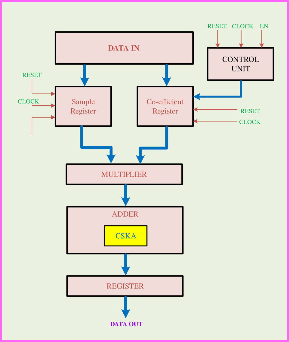
Figure 1. Block diagram of proposed method
The suggested architecture’s block diagram demonstrates how the data inputs are supplied as samples or as data for their register. The input data is stored in both sample and co-efficient register. The control unit block id used to enable the co-efficient register through enable input signal. If the coefficient data enable is set to high, the input coefficient value is transferred to the register. If the sample input enable is set to high, it uses the sample input values. Both functions rely on data inputs. The coefficient data and sample data are the inputs to the multiplier block. It multiplies the coefficients and transmits the results to adder circuit to do arithmetic operation of addition. One of the essential FIR filter blocks that determines the filter’s overall effectiveness in DSP applications including image, audio, and video processing is the adder. In order to decrease latency and circuit area, the Carry Skip Adder (CSKA) is added to this adder circuit. This suggested adder takes the carry bit if only carry bit generated in full adder result otherwise this adder skips the carry signal. Therefore, the speed of operation will increase and propagation delay will reduce as well. The individual operation of FIR and CSKA is discussed in following sections.
Finite Impulse Response (FIR) Filter
This filter is also known as non-recursive digital filters, is caused by the fact that they settle to zero after a predetermined period of time. Since there is no feedback in the FIR in the usual scenario, the impulse response is limited. The impulse response will always have a fixed size because there won’t be any feedback. The basic diagram of FIR filter is shown in Figure 2. A tap is the output of each register, and it is identified by the equation s(n), where n is the tap number. A constant termed h(n) is applied to each tap, and the resultant products are then added. The equation of FIR filter is expressed as follows:
y(n)= ∑n=1N(S(n) h(n)) (1)
The coefficients for a linear phase response FIR filter are symmetrical around the centre values. The symmetric taps can be added before they are multiplied by the coefficients due to this symmetry.
The output function of N-tap FIR filter with h(K) coefficient can defined from following expression:
y(n)=h(0)*S(n)+h(1)*S(n-1)+h(2)*S(n-2)………h(N-1)*S(n-N-1) (2)
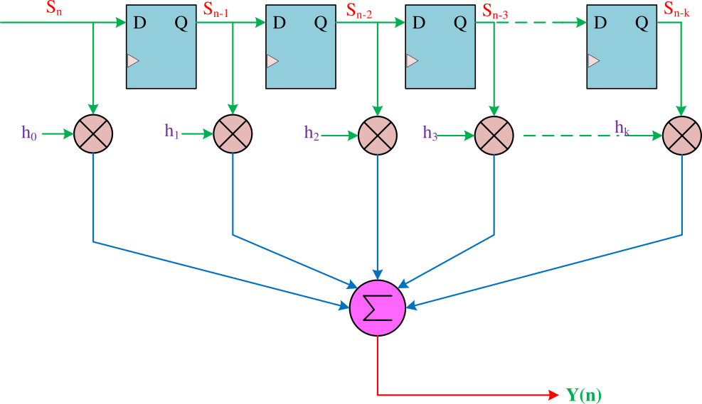
Figure 2. General Structure of FIR filter
Numerous methods, including as windowing, frequency sampling, and optimisation algorithms, are frequently used in the construction of FIR filters. Once the filter coefficients have been established, a convolution operation is utilised to filter the incoming data in real-time. FIR filters, which offer stability, adaptability, and exact control over their frequency response, are a key element of digital signal processing. For functions like signal conditioning, noise reduction, and frequency shaping, they are extensively employed in applications ranging from audio, video, image processing and communication systems. A FIR filter’s frequency characteristics can be set to low-pass, high-pass, band-pass, or band-stop. A FIR filter may also be linear phase in order to prevent skewing the input signal’s phase. The delay components, multipliers, and adders that make up an FIR filter combine to perform the convolution between the input signal and the filter coefficients. The filter coefficients scale and modify the filter’s frequency response.
In FIR filters, adders play a crucial role since they aggregate the partial products of the multiplication process and conduct the addition operation between input signal and filter coefficients. According to design and execution, adders can influence the speed, size, and power consumption of FIR. The main drawbacks of several types of adders, such as ripple-carry adders, carry-lookahead adders, carry-save adders are more propagation delay of time and thus the speed of operation reduced and, power consumption of filter design will increase. This research proposes Carry Skip Adder (CSKA) which can shorten the delay by omitting some carry bits, use less power and less space by utilizing fewer logic components. Therefore, CSKA for a particular FIR filter might increase its effectiveness and performance. This adder is discussed briefly in following section.
Carry Skip Adder
When compared to other adders, CSKA is a simple version of an adder that reduces ripple-carry adders’ latency. It is also referred to as a carry-bypass adder sometimes. The worst-case latency is reduced by merging many carry-skip adders into a block-carry-skip adder. The n-bit carry skip adder consists of an n-input AND-gate, an n-bit carry ripple chain, and a single multiplexer. The n-input AND-gate is connected to each of the propagation bits, pi, of the carry-ripple-chain. The resulting bit is used as a choice bit in a multiplexer, switching either the carry-in signal c0 or the last carry bit to the carry-out signal cout. With a group propagate signal set to logic 1, the carry bit for each block may now “skip” over blocks, dramatically lowering the latency of the adder through its critical route. As opposed to a lengthy ripple-carry chain, which would require the carry to ripple over each bit in the adder, this does not require this. The breadth of the adder is the same as the AND-gate’s input count. Wide widths make this more challenging and slow down the process since the AND-gate must be built as a tree. A acceptable breadth is reached when the sum-logic has the same depth as the n-input AND-gate and the multiplexer. Figure 3 displays the main block diagram of CSKA.
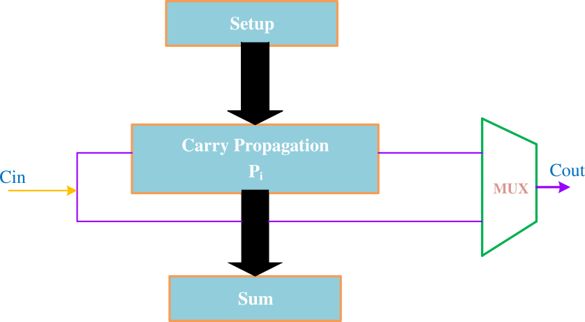
Figure 3. Simplified Block diagram of CSKA
InCSKA, the data that has to be added is divided into blocks of varied sizes. Each block’s carry and sum bit are produced via ripple carry. The primary idea behind carry computation, or skipping carry across groups of subsequent adder stages, is the basis for CSKA. Thus, this shortens the delay. The sum and carry Boolean expressions are as follows:
Carry Propagate (Pi)= Ai ⊕ Bi (3)
Sum (Si)= Pi+Cin (4)
Carry out (Ci+1)= AiBi+ PiCin (5)
It should be noted that if Ai = Bi then Pi = 0, which limits the dependencies of Ai and Bi; The important conditions of CSKA are given below:
If Ai = Bi= 0, then Ci+1=0
If Ai = Bi= 1, then Ci+1=1; else
If Ai ≠ Bi, then Pi= 1; and Ci+1= Cin
Therefore, for each Ai, Bi in a group or block, it is not necessary to compute the new value Ci+1. In this situation, the block’s carry-in (Cin) can be passed immediately to the following block. Carry will be produced and propagated up to that block’s output if Ai = Bi= 1. Carry will not be propagated by that bit position if Ai = Bi= 0. In order to enable the Cin to skip the block or group, the carry-skip adder first determines if all Ai and Bi are present in each group. Typically, there can be a difference between a block-skip delay and the propagation delay of a carry to the next bit position.
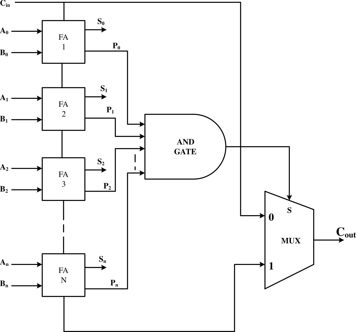
Figure 4. Basic structure of carry skip adder
Proposed Carry Skip Adder into FIR
This research proposed a novel integration of Carry Skip Adder into FIR for real time DSP applications. In conventional FIR filter might be suffer with more propagation delay due to adder circuit used in FIR filter. This paper introduces CSKA in FIR filter to reduce area, delay, and power dissipation. This proposed approach is more effective for real-time DSP applications since FIR filter is typically utilised in DSP applications including image, video, and audio processing. Figure 5 depicts the proposed carry skip adder’s circuit design.
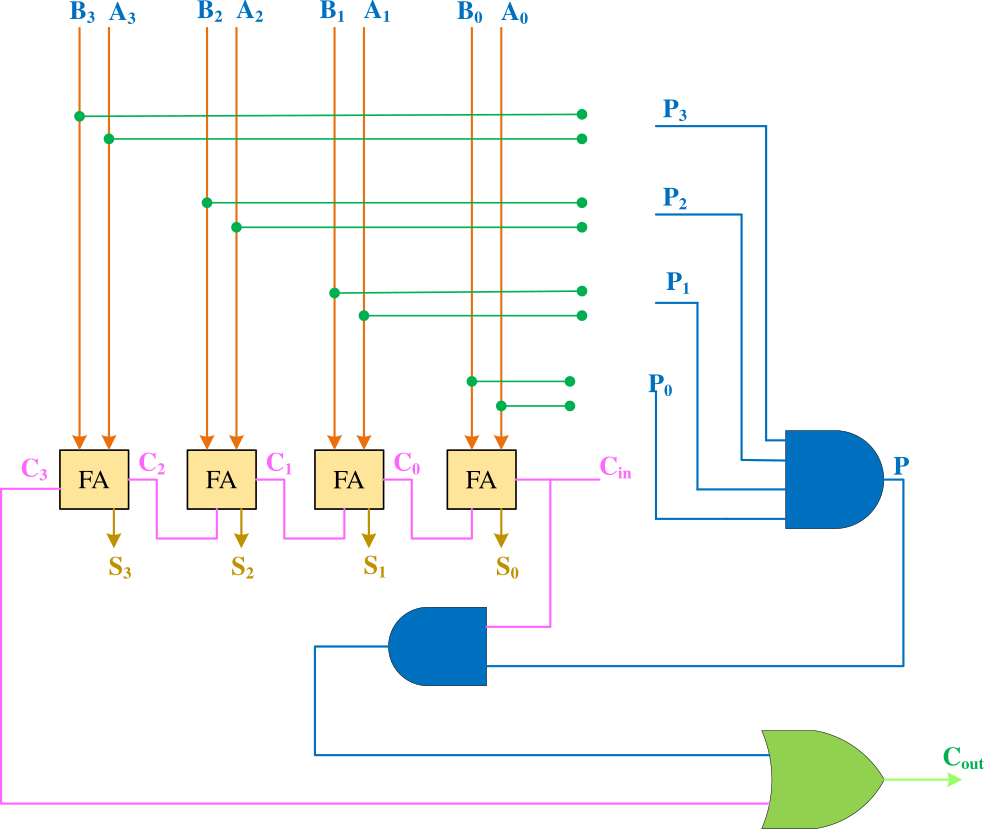
Figure 5. Architecture of Proposed CSKA
The n-bit CSKA is often divided into n/4 blocks, where n is a multiple of 4. Each block consists of four stages. The CSKA logic is implemented using a four XOR gate. All output of Exclusive OR gate is applied to AND gate. Four XOR gates are used to generate propagation signals (P0-P3). These developed propagating signals are given to AND for producing resultant signal. Four input AND gates and combine to form the propagate signal (P). Additionally, OR, AND gates work together to determine the carry bit’s ultimate value. The carry propagation method based on fusion of input vectors should be avoided in favour of reducing carry propagation delay. The time required for the longest carry propagation is minimised using a constant block size, where the ith carry propagation is designated as Pi. Therefore, the suggested method will produce less propagation delay. High speed of operation and it reduces the area as well. This proposed strategy is suitable for real time DSP applications.
RESULTS AND DISCUSSION
The suggested new integration of Carry Skip Adder in the Finite Impulse Response Filter, the most important component in applications of digital signal processing is presented in this section along with simulation and assessment results. The major goals of this newly created approach are to decrease power, area, and propagation delay. Using the Xilinx ISE 14.7 tool, the circuit design for suggested technique is synthesised and simulated.
Simulation Result of Carry Skip Adder
Initially, the CSKA is analysed for verify its performance. The time delay is the most important parameters to decide the operation of any digital circuit. This timing delay of the circuit will decide operating speed of circuit and it reduces the power consumption as well. Therefore, the CSKA is implemented and simulated using ISE simulator tool. Figure 6 displays the CSKA’s created RTL design, and Figure 7 illustrates the results of the simulation.
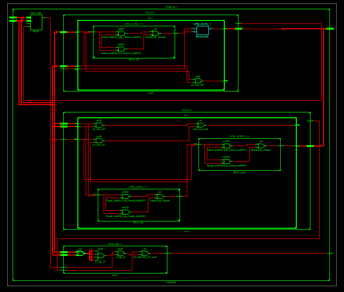
Figure 6. RTL schematic of Carry Skip Adder
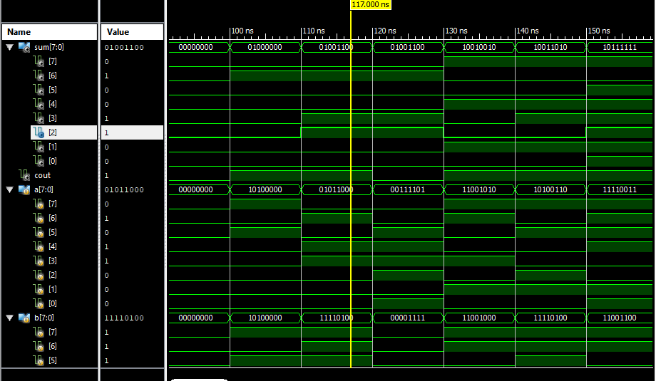
Figure 7. Simulation result of CSKA
In this proposed CSKA, XOR gates are used to generate the propagation signals and generated propagating signals are applied to and gate to produce resultant signal of propagation. It will generate the low signal if both the inputs applied full adder circuit are equal and it will produce high signal if inputs are unequal. Then resultant propagation signal and carry input are applied to AND gate to generate the signal and then the output of AND gate is given to OR gate. This gate combines this signal with carry out of last stage full adder circuit and produce carry output. The purpose of introducing propagation signal is to skip the carry bit if it is zero. Thus, the time delay will be reduced and also area, power of the circuit will be decrease. The technology schematic is shown in Figure 8.
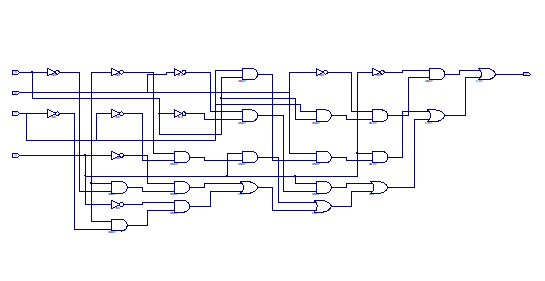
Figure 8. Technology schematic of CSKA
The timing constraint of CSKA is evaluated with simulation result. Gate delay, fanout, and net delay are analysed. All timing delay is mentioned in nanoseconds. The total time delay including, gate and path delay is indicated as 8.818 ns. The default path analysis of CSKA is illustrated in Figure 9.
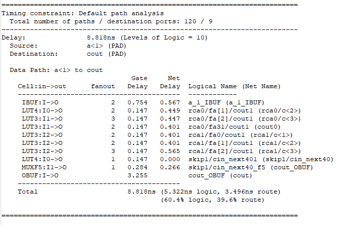
Figure 9. Analysis of Delay
Simulation Result of Proposed CSKA with FIR
In this research, the CSKA is suggested in FIR filter to reduce delay so that power consumption of circuit will be reduced. The FIR filter is applied in variety of fields. The crucial part of FIR filter is adder. This circuit will decide the performance of the system. The time delay will be more in traditional adder used in FIR. The benefit of carry skip adder is it will skip the carry if there is no carry generated in previous adder circuit. Thus, the delay of circuit is much less than that of conventional adder. The overall performance of the system will be more efficient when this recommended FIR with CSKA used in digital signal processing since it produce less time delay. Because of this advantage, the operating speed of processing unit of device will be more efficient. This proposed technique is synthesized and simulated using Xilinx ISE tool and simulation and RTL schematic of this circuit is displayeded in following Figure 10 and 11.
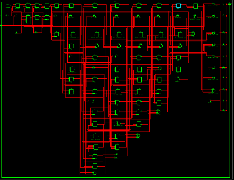
Figure 10. RTL schematic view of FIR with CSKA
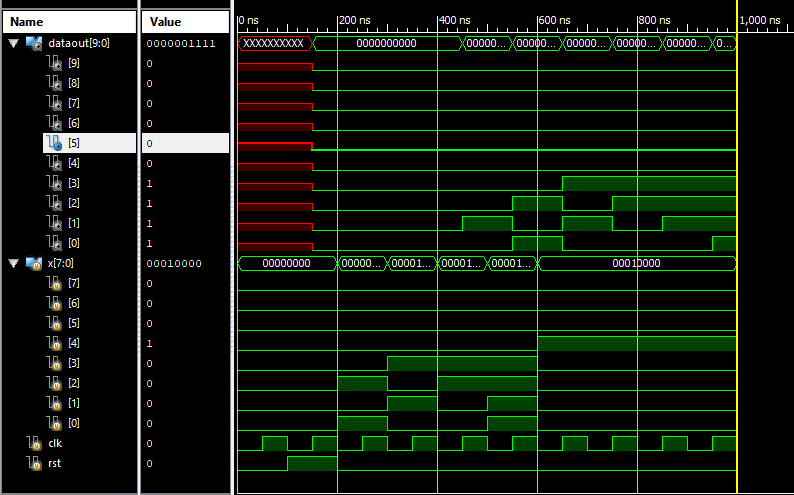
Figure 11. Simulation result of FIR with CSKA
CSKA is employed in a variety of computational framework designs to control the propagation delay brought on the carry, which is skipped to get the total over the carry blocks. The final carry and total of the CSKA are chosen by multiplexers. Since it skips null carry bits, the time delay, critical path delay will be reduced and this FIR filter with CSKA is more suitable for DSP applications. The timing summary and device utilization summary report are displayeded in Figure 12 and 13.
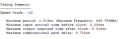
Figure 12. Timing Summary of Proposed method
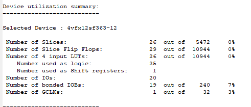
Figure 13. Device Utilization Summary of Proposed circuit
Comparison of proposed method with existing adders
In this section, the suggested method is compared with several types of existing adder circuits used in FIR filter. The main parameter of FIR filter in digital signal processing is time delay and frequency. These aforementioned metrics will decide the performance of system. Hence, the recommended CSKA is evaluated with various methods which are currently in practice. Table 2 illustrates the evaluation of FIR with CSKA and existing methods.
Table 2. Comparison Table
Methods | Time Delay (ns) | Frequency (MHz) |
CSLA | 6.16 | 373.65 |
HC-Hybrid | 7.1 | 392.55 |
CSA | 8.31 | 444.78 |
4:2 Compression Adder | 9.03 | 498.36 |
Proposed | 1.819 | 549.753 |
The suggested method is evaluated with existing techniques and obtained values are depicted in aforementioned Table 2. Graphs are plotted from these values for time delay and frequency and they are displayeded in Figure 14 and 15.
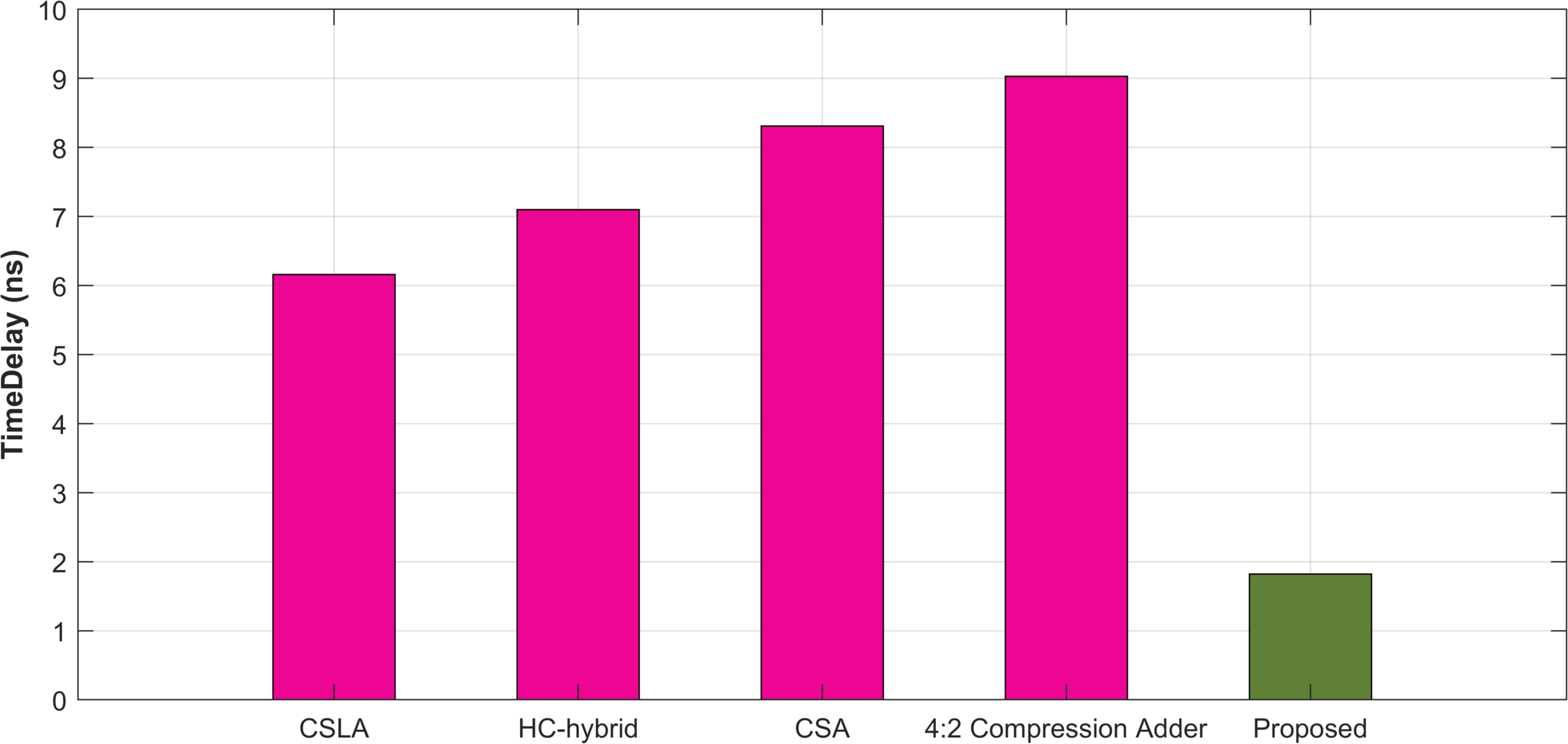
Figure 14. Time delay analysis
The above figure represents a time delay analysis of proposed and existing method. The graph was plotted from the values given in Table 2. The time delay of Carry Select Adder (CSLA), HC-Hybrid pipeline adder, Carry Save adder, 4:2 Compression adder, and proposed CSKA adder are 6.16 ns, 7.1 ns, 8.31 ns, 9.03 ns, and 1.819 ns respectively. This result shows that, the proposed adder circuit has the least time delay when compared to existing various adder circuits used in FIR filter. Therefore, the suggested circuit performs better than all other existing circuits.
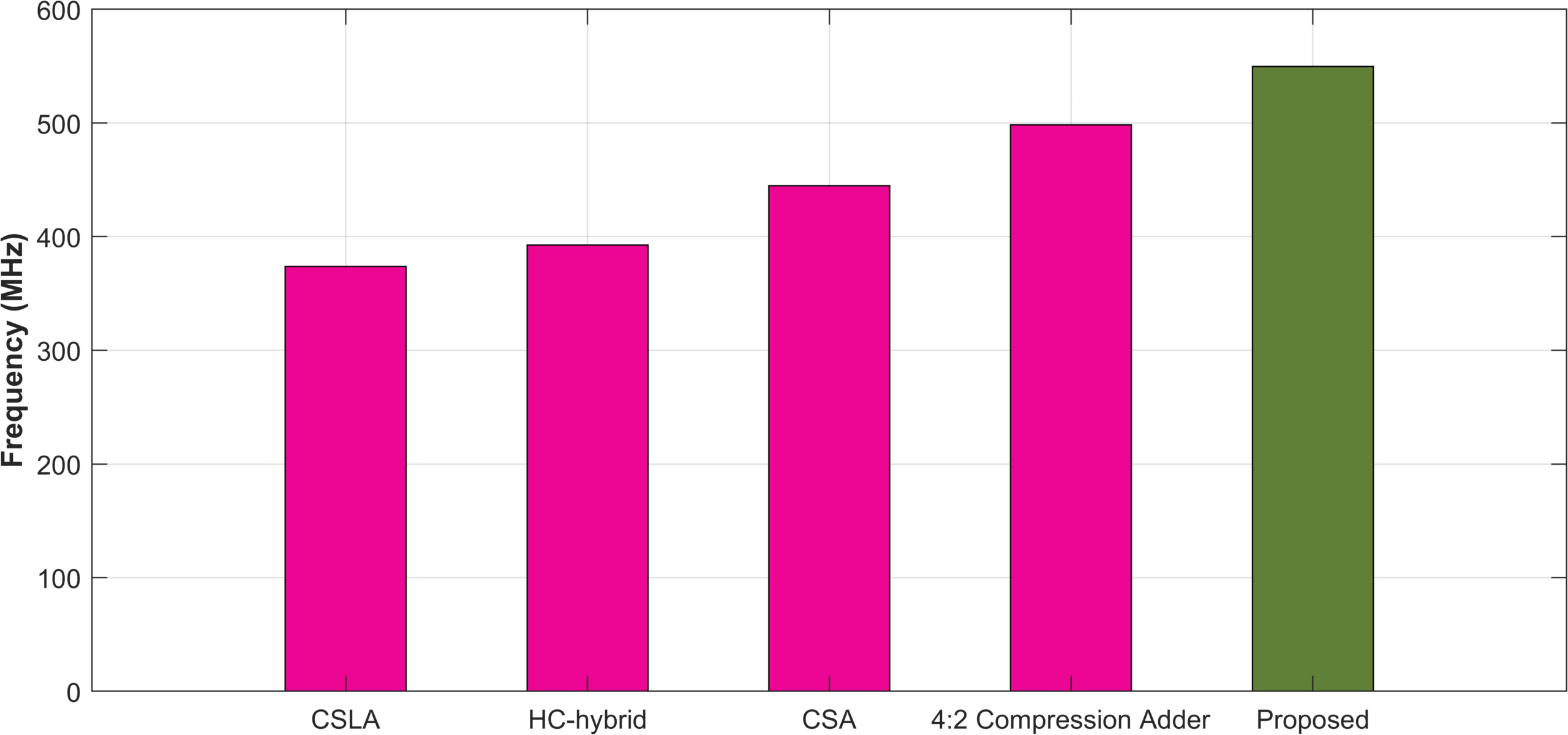
Figure 15. Frequency analysis
The aforementioned graph shows the frequency response of proposed CSKA circuit and various existing circuits. The frequency values are mentioned in MHz. The values are indicated as 373.65 for CSLA, 392.55 for HC-hybrid, 444.78 for CSA, 498.36 for 4:2 Compression Adder, and 549.753 for newly developed FIR with CSKA. These evaluations show that the recommended circuit has a higher frequency than all other existing adder circuits used in FIR filter. Since the proposed circuit has highest frequency with less time delay, this circuit will give great performance in all DSP applications.
Result of DSP signal with proposed circuit
In this section, the suggested FIR filter with CSKA circuit is applied to signal to verify the performance of proposed circuit. For this purpose, the reference signal was generated using MATLAB software and proposed filter is applied to developed signal. It gives good result and the difference of signal before and after applying FIR filter with CSKA is shown in following Figures 16 and 17. These figures clearly display the difference and the signals have more improvement after applying FIR with CSKA filter. Therefore, the proposed circuit is well suited for real time digital signal processing applications.
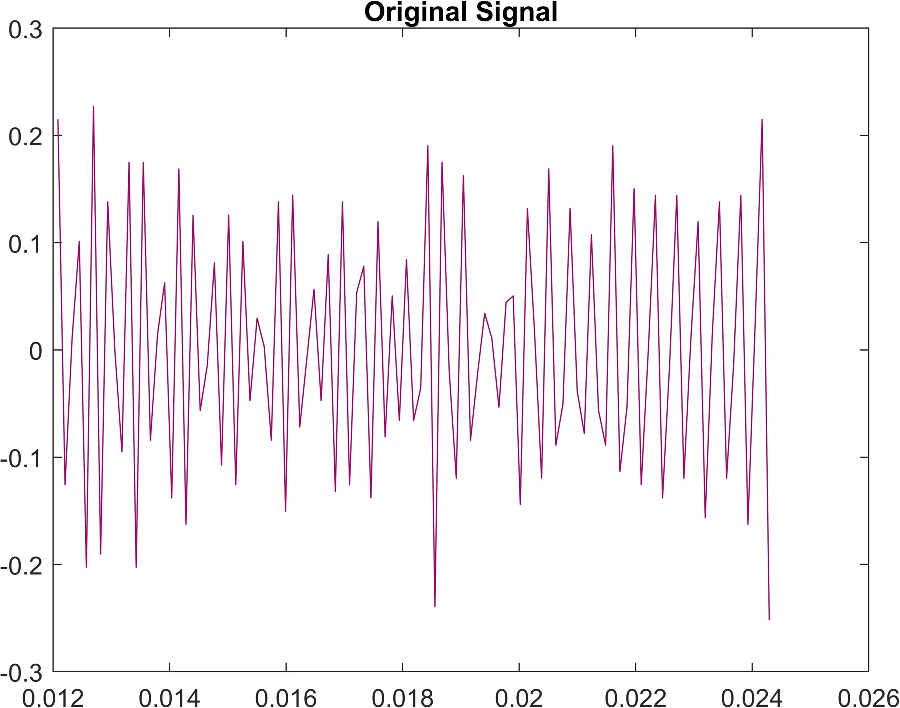
Figure 16. Original signal
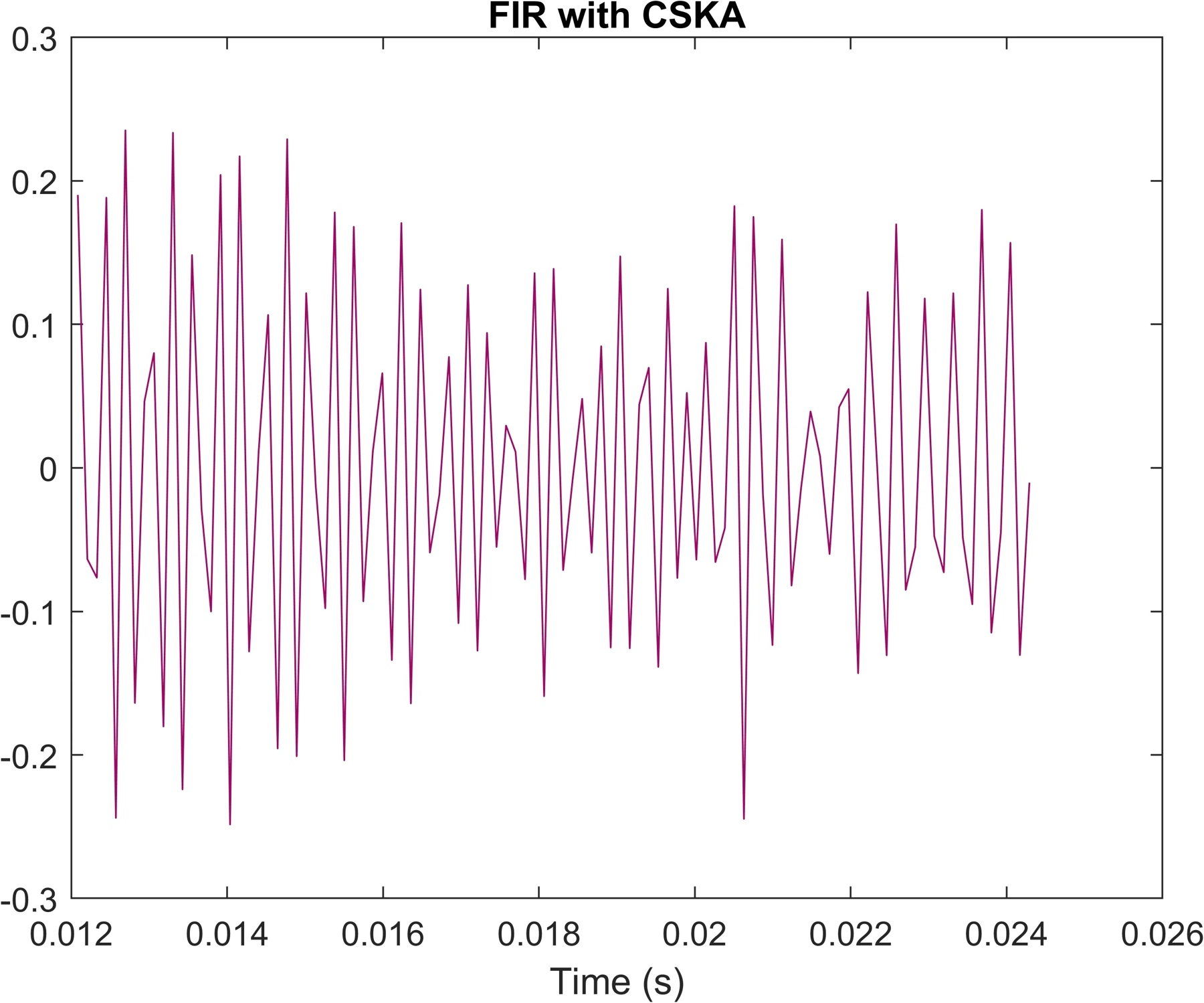
Figure 17. Signal with proposed method
CONCLUSION
This study introduced a carry-skip adder into a finite impulse response filter to reduce delay and improve performance. Compared with other adder circuits used in FIR filters, the proposed CSKA implementation produced a shorter delay by skipping unnecessary carry propagation. The circuit was synthesised and simulated using Xilinx ISE 14.7. The results showed improvements in delay and operating frequency, with a corresponding expected reduction in power consumption. Applying the CSKA-based FIR filter to a signal also demonstrated its performance. Reduced delay and increased operating frequency are the main benefits of the circuit. The proposed strategy can therefore be applied to digital signal processing applications that require low delay, low power consumption and high operating speed.
References
Wang, X.Y., Zhou, P.F., Eshraghian, J.K., Lin, C.Y., Iu, H.H.C., Chang, T.C. and Kang, S.M., 2020. High-density memristor-CMOS ternary logic family. IEEE Transactions on Circuits and Systems I: Regular Papers, 68(1), pp.264-274.
Saravana Ram, R., Gopi Saminathan, A. and Arun Prakash, S., 2020. An area efficient and low power consumption of run time digital system based on dynamic partial reconfiguration. International Journal of Parallel Programming, 48, pp.431-446.
Damaj, I.W., Yousafzai, J.K. and Mouftah, H.T., 2022. Future trends in connected and autonomous vehicles: Enabling communications and processing technologies. IEEE Access, 10, pp.42334-42345.
Brandt, A., 2019. A signal processing framework for operational modal analysis in time and frequency domain. Mechanical Systems and Signal Processing, 115, pp.380-393.
Karthick, R., Senthilselvi, A., Meenalochini, P. and Senthil Pandi, S., 2022. Design and analysis of linear phase finite impulse response filter using water strider optimization algorithm in FPGA. Circuits, Systems, and Signal Processing, 41(9), pp.5254-5282.
Martinek, R., Rzidky, J., Jaros, R., Bilik, P. and Ladrova, M., 2019. Least mean squares and recursive least squares algorithms for total harmonic distortion reduction using shunt active power filter control. Energies, 12(8), p.1545.
Qin, W., Gamba, M.T., Falletti, E. and Dovis, F., 2020. An assessment of impact of adaptive notch filters for interference removal on the signal processing stages of a GNSS receiver. IEEE Transactions on Aerospace and Electronic Systems, 56(5), pp.4067-4082.
Raju Kalidindi, S.N., Terlapu, S.K. and Krishna, M.V., 2021. Implementation of efficient reconfigurable FIR filter with control logic for 5G applications. Soft Computing, 25(15), pp.10509-10518.
Li, L., Chen, Z., Aphale, S.S. and Zhu, L., 2020. Fractional repetitive control of nanopositioning stages for high-speed scanning using low-pass FIR variable fractional delay filter. IEEE/ASME Transactions on Mechatronics, 25(2), pp.547-557.
Ramesh, A.V., Kumar, A.R., Iyengar, A.S. and Yadav, L., 2020. Implementation and Design of FIR Filters using Verilog HDL and FPGA. Perspectives in Communication, Embedded-systems and Signal-processing-PiCES, 4(5), pp.85-88.
Cho, S.M., Meher, P.K., Trung, L.T.N., Cho, H.J. and Park, S.Y., 2021. Design of very high-speed pipeline FIR filter through precise critical path analysis. ieee access, 9, pp.34722-34735.
Sarma, R., Bhargava, C., Jain, S. and Kamboj, V.K., 2021. Application of ameliorated Harris Hawks optimizer for designing of low-power signed floating-point MAC architecture. Neural Computing and Applications, 33, pp.8893-8922.
Saravanan, S. and Poovarasan, R., 2022. FPGA Implementation of FIR Filter Using Approximate Computing. Journal of Algebraic Statistics, 13(3), pp.4130-4136.
Amirsoleimani, A., Alibart, F., Yon, V., Xu, J., Pazhouhandeh, M.R., Ecoffey, S., Beilliard, Y., Genov, R. and Drouin, D., 2020. In‐Memory Vector‐Matrix Multiplication in Monolithic Complementary Metal–Oxide–Semiconductor‐Memristor Integrated Circuits: Design Choices, Challenges, and Perspectives. Advanced Intelligent Systems, 2(11), p.2000115.
Pazhani, A.A.J. and Vasanthanayaki, C., 2019. Design and Implementation of Computationally Efficient Arithmetic Unit. Journal of Electrical Engineering, 19(3), pp.9-9.
Patali, P. and Thottathikkulam Kassim, S., 2019. High throughput FIR filter architectures using retiming and modified CSLA based adders. IET Circuits, Devices & Systems, 13(7), pp.1007-1017.
Arun Sekar, R. and Sasipriya, S., 2019. Implementation of FIR filter using reversible modified carry select adder. Concurrency and Computation: Practice and Experience, 31(14), p.e4952.
Shah, S. and Rajula, S., 2019. Design of FIR filter architecture for fixed and reconfigurable applications using highly efficient carry select adder. In Soft Computing and Signal Processing: Proceedings of ICSCSP 2018, Volume 2 (pp. 627-637). Springer Singapore.
Rammohan, S.R., Jayashri, N., Bivi, M.A., Nayak, C.K. and Niveditha, V.R., 2020. High performance hardware design of compressor adder in DA based FIR filters for hearing aids. International Journal of Speech Technology, 23, pp.807-814.
Sravani, K. and Rao, R., 2020. Design of high throughput asynchronous FIR filter using gate level pipelined multipliers and adders. International Journal of Circuit Theory and Applications, 48(8), pp.1363-1370.
Kannan, L.M., 2021. A Design of Low Power and Area efficient FIR Filter using Modified Carry save Accumulator Method. Turkish Journal of Computer and Mathematics Education (TURCOMAT), 12(7), pp.1735-1750.
Sakthivel, R. and Ragunath, G., 2021. Low power area optimized and high speed carry select adder using optimized half sum and carry generation unit for FIR filter. Journal of Ambient Intelligence and Humanized Computing, 12, pp.5513-5524.
Sathyakala, M.D., Mathumat, M.M., Priya, M.T.D. and Deepika, M.S., 2021. An efficient fir filter design using three-operand binary adder. Int Res J Eng Technol, 8(3), pp.3166-3171.
Mandloi, A. and Pawar, S., 2021. Power and delay efficient fir filter design using ESSA and VL-CSKA based booth multiplier. Microprocessors and Microsystems, 86, p.104333.
Kumm, M., Volkova, A. and Filip, S.I., 2022. Design of optimal multiplierless FIR filters with minimal number of adders. IEEE Transactions on Computer-Aided Design of Integrated Circuits and Systems, 42(2), pp.658-671.
Cite This Work
To export a reference to this article please select a referencing stye below:

Academic Master Education Team is a group of academic editors and subject specialists responsible for producing structured, research-backed essays across multiple disciplines. Each article is developed following Academic Master’s Editorial Policy and supported by credible academic references. The team ensures clarity, citation accuracy, and adherence to ethical academic writing standards
Content reviewed under Academic Master Editorial Policy.