Introduction
In the era of Digital Transformation and Intent-based networking, high-end line cards are getting heavier and denser regarding circuitry and discrete numbers. As per extensive experimental tests done at <suppressed> laboratory, it is found larger size footprint ASICs have lower maximum allowable principal strain and strain rates on the PCB (<suppressed> 2016) and are more susceptible to JTAG (commonly referred to as boundary-scan and defined by the Institute of Electrical and Electronic Engineers (IEEE) 1149.1) failures due to Ball grid array (BGA) brittle fracture at component side or board side when subjected to mechanical shocks. In several studies, including random vibration reliability of BGA by Fang Liu et al. (2014) reports, the propagation rate of cracks in solder joints increases as ASD (Acceleration spectral density) increases. There are several reasons for a solder joint to fail (T. Simo et al. 2015, Li. W 2017), including mechanical stress. An example of such field failures of <suppressed> Mechanical Design Verification Test (MDVT) and <suppressed> Packaging Test passed card is <suppressed> Series <suppressed> Gigabit Ethernet line card. Around <suppressed> cards were field returned during <suppressed> and it was root caused by NPU device BGA failures on many of these cards irrespective of device location on the PCB.
Mechanical Design efforts to mitigate the field failure were such as reducing the heatsink weight on the ASIC and adding multiple stiffener points on the heatsink, etc. However, it was not affirmative for the project team about the exact location and time of these card failures, and intense mechanical shocks were anticipated to be the probable cause of failure. Printed Circuit board, electrical components, and Heatsinks on the line cards consist of approximately 80% of the overall card weight. Most of the advanced cards are over <suppressed> lbs. in weight, and this contributes to higher energy conversion and transfers to the PCB in the event of a drop or shock load. The line cards are inherently fragile at the component side of BGA on a device. Hence it is important these sophisticated and expensive cards are handled with utmost care both in packaged and unpackaged conditions, i.e., during transportation and in use condition. Hence a project proposal is made to integrate the required circuitry on to the boards with the help of <suppressed> Hardware and Software Engineering team and the paper focus on resources required to implement the proposal.
Research Aim & Objectives Aim:
- Integrate Mechanical Shock and Vibration Logger circuitry on the Telecom card motherboard
- Expose perpetrators of damage due to mechanical shock and reduce the number of field returns of expensive cards due to mechanical shock-related failures.
Objectives:
- Work with <suppressed> Hardware and Software Engineering to implement the proposal
- Perform laboratory tests and transportation tests to various locations to validate the integrated hardware performance and software readings.
- Collect the field test data and analysis to make necessary changes to the Mechanical Design Verification Test and packaging test plans and thresholds if required.
- Trace physical locations of field failures and provide quantitative data to take preventive actions
- .Provide necessary insight to management on field failures of cards due to shock and vibration
- Make available the measured data in case of warranty claims due to mishandling
Research Hypothesis
Integrating Shock data logger circuitry on the main board will reduce the field return of expensive Line cards.
Literature Review
A wide range of external influences during transportation could lead to the goods becoming damaged. After the card is out of the packaging, there are possibilities of unpackaged shocks and vibrations when the card is handled to insert into a chassis or taken out to replace it. Most of the time, the failed and returned cards are sent back from a customer site to a depot or <suppressed> labs without the original package. This also accounts for cards being subject to unpredictable shock levels. There are miniature-size battery-operated shock logger devices commercially available in the market, and they are being used in different industries such as automation, industrial goods, machine engineering, Aeronautics, aerospace industry, agricultural technology, Sport, leisure, etc. and many others. Most of these thumb-sized circuitry boards use piezoelectric, Piezoresistive, capacitive MEMS (micro-electro-mechanical systems) technologies accelerometer, and it could read +/- 2g up to 2000g or more levels of acceleration. Additionally, commercial data loggers are also capable of reading temperature, humidity, pressure, light, etc. Software to read and analyze data logs is also provided. “A 900 mAh lithium-polymer battery unit could ultimately monitor the acceleration over a period of up to six months, provided the measurement frequency was appropriately adjusted” as per MSR a Swiss made data logger device manufacturer.
These commercially available data loggers (Steve Hanly, 2017) are expensive and not practical to be used as a commodity item that goes along with each <suppressed> board with a <suppressed> Year warranty. Integrating the circuit on the Mainboard eliminates the accelerator mounting methods and the influence of natural frequency shift. Also, external sensor wiring, ground loops, a risk of a loose connection, etc., are eliminated.
The data logger has four types of input channels: output, digital, remote and virtual. The data recorder receives data directly from the corresponding inputs are analogical and digital channels. Remote routes are received with the Modbus RTU protocol, which acts as a master in the RS485 interface. The virtual channels are a special type of input channels that allow you to perform mathematical operations and calculate complicated formulas for the measured information. Analog input channels can be configured to read voltage, current, dermopathy, Pt100, and Pt1000. These inputs are based on 24-bit A / D converter accuracy with a high data rate of data, which can reach 1000 samples per second. Digital channels can be individually configured as inputs or outputs.
The Ethernet interface allows you to download data and access inputs and outputs through services that can be enabled and configured individually. Through a web browser (HTTP), it can show the active data, diagnostics and general data of the Data Logger. The FTP client can be used to register data. The data logger can configure 32 different alarm states that begin the output when the alarm condition is detected, allowing you to send emails or SNMP traps. All information about the variables, status, and diagnostics of the Data Logger can be used in Modbus records available through the Modbus TCP interface or Modbus TCP interface or working through the USB (device) or RS485 (available) interface. Expensive).
The USB interface device is used to connect to the configuration, monitoring or download of the computer. The host USB interface is used to connect a USB flash drive to download details of the registration memory. Data logging can be transferred to the configuration software with any of the interfaces that allow you to export a wide variety of data formats. The DISPLAY can install or install color GUI (Human Machine Interface) remotely (optional) when the data measured from the process must be displayed. Shock is typically considered a short-duration event with large magnitude acceleration often expressed as G level, where 1G= 9.81 m/s2. According to accepted theory (N. Robert, 1968), an impact shock pulse to a product must have a velocity change and a critical deceleration for a component inside the product to fail. The chassis of these cards are made of pre or post-plated carbon steel or anodized Aluminum cover, carrier and faceplate. The size of the line/fabric cards is driven in most cases by the size of the printed circuit board and the system into which it gets installed. On a typical board, the main ASICs are x 55 mm, 55 x 55 mm or 35 x 35 mm size in length and width. With the introduction of lead-free solder alloys, brittle fracture failures have increased (B. Sykes,2005). Mechanical design robustness and design margin are validated during <suppressed> MDVT. However, when all test-passed equipment fails in the field at a component level, it is imperative for the Mechanical and Hardware Engineering team to find out the cause.
<Suppressed> Hardware, Software, Mechanical Engineering and Electrical CAD (ECAD) resources are required to implement the proposal. The hardware engineering team selects the required sensor (Refer to Table 1) and circuitry components meeting <suppressed> reliability rating and other requirements and provides necessary circuitry schematics to ECAD. ECAD engineer allocates the space and places the components on the board considering all PCB manufacturing guidelines and rules. Mechanical Engineer participates in the overall project cycle from feasibility, MCAD-ECAD IDF verification through implementation testing.
To read the data log, the software engineer does the necessary coding and compiles it to a <suppressed> operating system.
Software main features to include:
- Statistics: FFT & Spectrograms generated for every sensor channel. Absolute maximum, minimum, as well as sampling rate and range of each sensor channel
- Logger Configuration: Configure the sampling frequency, Calender wake, time delay, recording duration and g-Level Triggers
- Export Data: Ability to export all data in CSV format for use with MS Office Excel, MATLAB, Python or any other analysis software packages.FFT and Spectrogram are exportable, and the time range of exported data is user-selectable
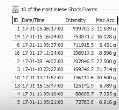
- Translate the shock events into a simple graphical representation of Acceleration levels on the Y-axis and date, a time stamp on the X-axis and PSD vs. Frequency Plots
Data Logger recommended: high-level Hardware specification Table 1
| Acceleration Range | ±2 to ±200 G (Tri-Axial) | |
| Sampling Rate: Maximum | Minimum | 10 kHz | 100 Hz | |
| Frequency Response Within ±5% Accuracy (X,Y & Z Axis) | 5 Hz to 1000 Hz | |
Transverse Sensitivity | < 10% | |
| Low-Pass Filter | 5th Order Hardware Butterworth (Linear Phase & Software Tunable) | |
| Natural Frequency | Bandwidth 0 to 1000 Hz | |
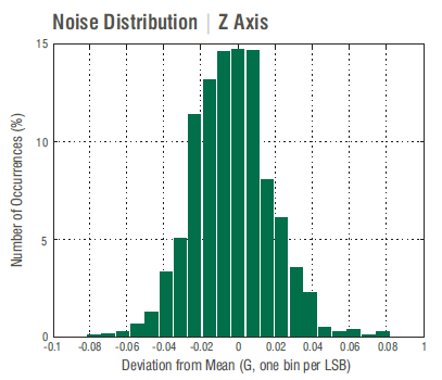
| Noise Density | 430μg/√Hz for Z-Axis, 290μg/√Hz for X, Y Axis | |
| Resolution | 16-bit | |
Battery | Rechargeable lithium polymer battery 900 mAh | |
| Memory Capacity | Over 2 000 000 measurement parameters | |
| Measurement rate | One /s to every 12 h | |
Research Design
Quantitative methods like experimental laboratory tests, real-time transportation tests and Qualitative methods of data collection such as personal experience and engagement are used to validate the circuitry on boards regarding shock response and data logging efficacy. Mechanical Fragility Test is performed to determine Critical Velocity change and Deceleration of the Board and to plot the damage boundary. The mechanical and Packaging engineers discuss and agree upon the locations where the shipping package will be in contact with and support the board during shipping. A fixture is designed to retain the unit on top of the test table to orient the product in the test direction axes. An accelerometer is attached to the board to measure the unit’s response acceleration to a specified input acceleration. The board is subjected to a Critical Velocity change step test as per ASTM D3332 Method A to meet the target maximum input velocity. The board is tested to find the Critical deceleration as per Table 4 with target maximum velocity change set to 2X critical obtained from the Critical Velocity change test.
Mechanical shock and Vibration tests are mentioned in Table 5 below as a part of <suppressed> Mechanical Design Verification test plan. <Suppressed> test accelerometer and data acquisition equipment (Lansmont Corp, Test Partner) are used to calibrate and validate the data logs of Integrated circuitry during operational tests. The results are tabulated to identify packaged and unpackaged shock and vibration levels. After laboratory tests, the units with integrated shock logger circuitry are physically shipped to different locations. A similar study was conducted by the University of Bern under “The use of MSR165 Data Loggers in a CTI research project.” The unpackaged units are distributed to <suppressed> labs to quantify the handling mechanical shock levels. On a return of the unit, the data readings are studied for severance of shock environments. Data is analyzed to find any gap in <suppressed> MDVT test plans. Product design changes are considered if required to dampen any damaging vibration frequencies.
Expected Outcomes
Nonoperational shock Experimental tests conducted in <suppressed> labs using Miniature STMicroelectronics (ST, 2018) data logger prototype show promising results. Although fairly inconsistent acceleration values were documented between the ST logger and <suppressed> MDVT accelerometer readings during the laboratory test, the wave patterns remained identical. It is found the miniature circuit is robust enough to withstand higher G level shocks, for example, packaged 36” height drop. The module can log date, time, year and G Levels.
ST logger Prototype image, <suppressed> Confidential
There are important factors that determine how the shock event is transmitted to the electronic device. The primary factors are drop height, type of impact surface, and product materials and configuration of Components within the product. Often One degree of freedom model (one DOF) is restricted in just a vertical free drop direction. It allows a simple and straightforward solution to be made for subsequent analysis. In summary, common assumptions used are:
- One DOF model of a spring-mass-damper is used
- The chassis is infinitely rigid
- Shock pulse is transferred directly to the component of concern inside the product
- .A device under Test (DUT) is in fully assembled condition
- The shock pulse response is the half-sine wave.
Circuitry Location on Board:
It is important to determine the location of the Circuitry on the board. An ideal location would be close to large-size ASICs. Data logger readings could be misleading if the circuitry is placed on a mechanically unsupported PCB location.
![]()

![]()
![]()
Battery: As per test results, it is found ST logger battery did not last as claimed. <suppressed> Hardware engineer would select the required sensor and battery for a longer duration of data logging during nonoperational shocks and keep the battery recharged whenever the card is plugged into the system.
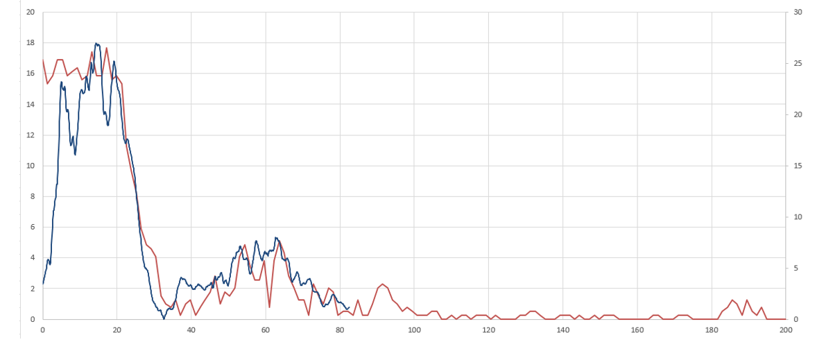
Memory: <suppressed> Hardware Engineer will determine the required memory size for the application. Software Readouts: Software readouts to be simple and intuitive to display the data log as graphs of Acceleration as a function of time stamps and Number of occurrences vs. G levels. See below the Examples of MSR data logger, Mide Shock & Vibration Accelerometer Loggers Cost: ST logger quotes (budgetary) unit price of <suppressed> based on <suppressed> EAU. Incorporating logger circuitry cost will be embedded in the NPI development budget, and it is estimated to be less than $10 per board based on ST prototype cost data points. Compliance Review: The circuitry will be reviewed by <suppressed> Compliance engineering team for Safety and EMI/EMC compliance.
![]()
![]()
![]()


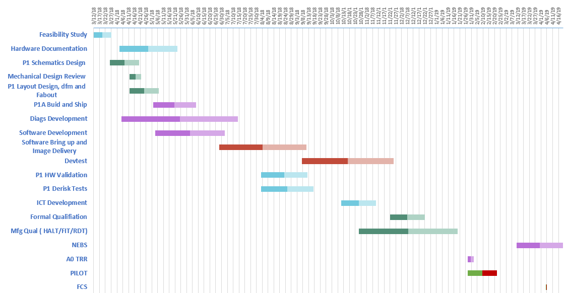
Project Plan

References
Newton, E. Robert., 1968, Fragility Assessment of Theory & Test Procedure, US Naval Postgraduate School
Lansmont Corporation, Test Partner.,2018, http://www.lansmont.com/products/test-partners, accessed on 9 April 2018
<Suppressed>., 2016, BGA Mechanical Shock Analysis, Presentation: <suppressed> Internal & confidential
Fang Liu, Guang Meng., 2014, Random vibration reliability of BGA lead-free solder joint, Journal: Microelectronics Reliability, Volume no: 54, Issue no: 1, pp- 226-232, DOI: 10.1016/j.microrel.2013.08.020
Daniel Klein, Gabriela Zumkehr., 2018, MSR data logger: small format all-rounders, Web page: https://www.msr.ch/en/fields-application/, accessed on 9 April 2018
Steve Hanly .,2017, Accelerometers: Taking the Guesswork out of Accelerometer Selection, Article, https://blog.mide.com/accelerometer-selection?utm_source=case-study-navair&utm_medium=case- study&utm_campaign=link-from-navair-case-study-to-accel-blog&utm_content=link-from-navair-case- study-to-accel-blog-10032016, Assessed on 9 April 2018
Bob Skyes., 2005, Testing for BGA Resistance to Brittle Fracture, Advanced Packaging July 2005, pp:38-41
Tsebo Simo, G.L.Shirangi, H.Nowottnick, M.Rzepka, S .,2015, Effects of board design parameters on failure mechanisms of PCB/BGA assemblies under drop impact 2015, 2015 IEEE 65Th Electronic Components And Technology Conference (ECTC), Electronic Components And Technology Conference (ECTC) , 2015 IEEE 65Th, p. 2048, IEEE Xplore Digital Library, EBSCOhost, viewed 9 April 2018.
Li, Weiming Sun, Xiaowei.,2017, An analysis case on the failure of BGA solder joints 2017, 2017 18Th International Conference On Electronic Packaging Technology (ICEPT), Electronic Packaging Technology (ICEPT), 2017 18Th International Conference On, p. 731, IEEE Xplore Digital Library, EBSCOhost, viewed 9 April 2018.
ST Microelectronics (2018), Website http://www.st.com/content/st_com/en.html, viewed 9 April 2018.
Cite This Work
To export a reference to this article please select a referencing stye below:
Academic Master Education Team is a group of academic editors and subject specialists responsible for producing structured, research-backed essays across multiple disciplines. Each article is developed following Academic Master’s Editorial Policy and supported by credible academic references. The team ensures clarity, citation accuracy, and adherence to ethical academic writing standards
Content reviewed under Academic Master Editorial Policy.
- Editorial Staff
- Editorial Staff
- Editorial Staff


